Introduction
Boolean Algebra
The Number System
BCD
BCD (Binary-Coded Decimal)
Classic method: 8421BCD.
add calculation:
the problem of carry:
$$ (14)_D+(28)_D=(0001\ 0100)_{BCD} + (0100\ 0100)_{BCD}\\ =(0101\ 1100)_{BCD}=(0110\ 0010)_{BCD} $$Gray Code
used in logic simplification and signal transmission.
every time a single bit is changed.
Floating poing Number
Negative numbers
Complement Numeric System
1’s Complement: $N_{1's} + (-N)_{1's} = (111...)_{1's}$ , or just inverting every bit of N. Low space efficiency and difficult to compute.
2’s Complement: $N_{2's} + (-N)_{2's} = (000...)_{2's}$ , or just inverting every bit of N and plus 1. A shift on 1’s Complement.
MSB=Most significant bit, LSB=Least significant bit.
$$ -N=N_{us}-2^n=\sum_{i=0}^{n-1}k_i2^i-2^n=-k_{n-1}2^{n-1}+k_{n-2}2^{n-2}+\dots k_02^0 $$So just set the weight of MSB to $-2^{n-1}$ .
we ignore the bit beyond the range to make sure the answer is correct.
$$ (101)_{2's}+(001)_{2's}=(110)_{2's}\\ (011)_{2's}-(001)_{2's}=(011)_{2's}+(111)_{2's}=(010)_{2's} $$To detect an overflow, we can notice if 2 positive numbers add up to a negative numbers or 2 negative numbers add up to a positive numbers.
We can fix overflow by adding 0 as MSB if the answer should be positive and adding 1 as MSB if the answer should be negative.
Boolean expression
Definition
$$ +(\text{OR/logic add}),\cdot (\text{AND/logic multiply}), \prime(\bar{})(\text{NOT/logit NOT}) $$Boolean function
Duality
AND<->OR, 0<->1, variables unchanged.
$$ F_1=F_2\Leftrightarrow F_1^D=F_2^D $$De Morgan’s Law
AND<->OR, 0<->1, X<->X’
Useful Theorem
X(Y+Z)=XY+XZ
XY+Z=(X+Z)(Y+Z)
X+XY=X
X(X+Y)=X
Boolean function simplification
2-level logic
Standard form
SOP and POS
Sum of Products or Products of Sum
Min-term
A min-term is a product of all variables taken either in the direct or complemented form, each variable shown once.
Max-term A max-term is a sum of all variables taken either in the direct or complemented form, each variable shown once.
$A+B+C=M_0$ and $A'+B'+C'=M_7$ $$ m_6= \overline{M_6} $$Karnaugh Maps
Use row and columns to represent combinations of the inputs(by min-terms), the cell to represent the value. The inputs is ordered by the sequence of Grey Code.
Simplification of 2-level logic
Karnaugh Maps method
If two adjacent min-terms deliver logic 1, merge them.
Implicant
$$ G\Rightarrow F, \text{then }G\text{ is the implicant of }F\\ no\ Q\ s.t.P\Rightarrow Q\Rightarrow F, \text{then }P \text{ is the prime implicant of }F\\ \text{If one min-term can only be covered by one prime implicant, this prime implicant is an EPI.} $$EPI will finally exist there.
Q-M method
algorithm to simplify multiple-input large-scale function.
Combinational Logic
Gate
NAND, NOT, NOR is better than AND, OR in saving area.
Transmission Gate Use both NMOS and PMOS to form a CMOS switch. NMOS is good at transmitting low volt while PMOS is better at working on high volt.
Tri-state Gate EN is high, TG on, F=A; EN is low, TG off, F is isolated from input A. The states are called logic 0, logic 1 and high-resistance Z.
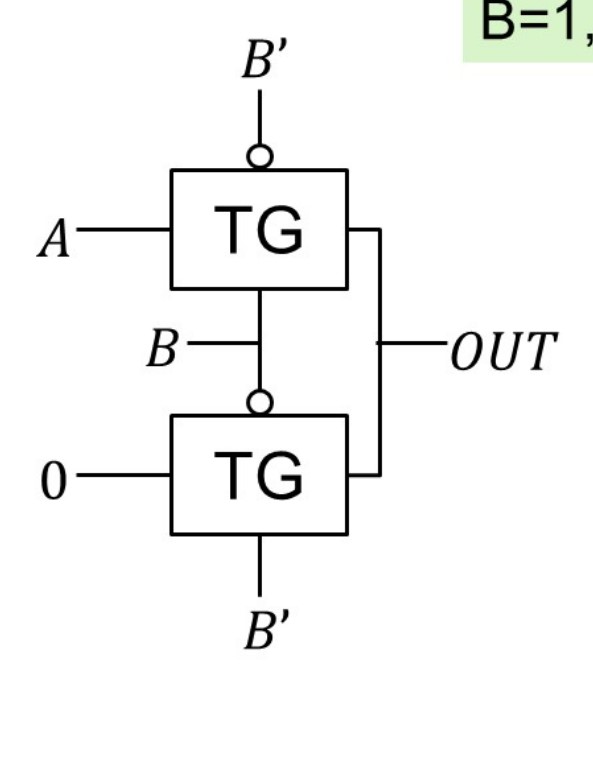
The bottom part of the circuit is used to avoid the high-Z state.
Combinational logic circuits
Outputs are the function of logic input circuits.
Determined only by current not past inputs + delay
To deal with complex logic with many inputs, we should:
- From 2-level to multi-level(BDD?)
- Divide-and-conquer
- Re-using
Metrics
Static metrics Logic voltage values, DC noise margins, Area, Fan-out
Dynamic metrics Speed/delay, Power dissipation, Noise(reference)
Speed rise time and fall time. Propagation time.
Fan out The maximum number of CMOS inputs that one logic output can drive.
Power and energy Leakage power(static power): subthreshold leakage power, gate leakage, D/S subtrate leakage. We can reduce the static power:
- increase $|V_{TH}|$
- or decrease $V_{DD}$ .
Dynamic power $P_{dynamic\_short}$ shows in pull-up and pull-down on.
$$ P = C_LV_{DD}^2\underset{\text{Flip Prob.}}{\alpha_{0-1}}f $$To reduce dynamic power:
- Reduce VDD and Capacitors
- Reduce frequency, flipping probability.
Energy-delay product is a metric. It’s hard to reduce.
- Low power can increase the lifetime of the chip.
- Low delay can increase the speed of the chip.
Hazard
static-1 hazard ‘1’ output has a transient ‘0’ glitch
static-0 hazard ‘1’ output has a transient ‘0’ glitch
dynamic hazard several transitions during a single output change(not required)
If the initial input and final input cannot be covered by one PI, it may have a glitch as state transition.
Basic comb. logic circuits
Encoder: inputs are more, outputs are less( $n \le 2^m$ )
Decoder: inputs are less, outputs are more( $m = 2^n$ )
Multiplexer: From several inputs, choose one as output according to the address inputs. It can be used to make a shift register. We can use n-bit-addr MUX for m-bit function.
Adder: Half adder & full adder.
Half Adder: $S = A \oplus B$
Full adder: $C_{out} = A\cdot C_{in} + B\cdot C_{in} + A\cdot B, S = A\oplus B\oplus C_{in}$
Implements of Full Adder:
Serial Adder $C_{i+1} = A_iC_i+B_iC_i + A_iB_i$ . The latency is disastrous.
Carry Lookahead Adder(CLA)
First define $P_i = A_i\oplus B_i, G_i = A_iB_i$ , P means Carry-bit propagation, G means Carry-bit Generation. Thus, $C_{i+1} = G_i + P_iC_i, S_i = A_i\oplus B_i\oplus C_i = P_i\oplus C_i$ . Thus the $C_i$ can be replaced:
$$ C_1 = G_0+P_0C_0\\ C_2 = G_1 + P_1(G_0+P_0C_0) = G_1 + P_1G_0+P_1P_0C_0\\ C_3 = G_2 + P_2(G_1 + P_1G_0+P_1P_0C_0) = G_2 + P_2G_1 + P_2P_1G_0+P_2P_1P_0C_0\\ C_4=G_3+P_3(G_2 + P_2G_1 + P_2P_1G_0+P_2P_1P_0C_0)=G_3+P_3G_2 + P_3P_2G_1 + P_3P_2P_1G_0+P_3P_2P_1P_0C_0 $$A 4-bit CLA can be designed using these formulas. For more, it is too complex. However, we can cascade the 4-bit CLA to reach the balance of latency and complexity.
Moreover, here comes the parallel intra- and inter-group CLA which regards the 4-bit adder as a block and defines its $P_i$ and $G_i$ , connecting the 4-bit adders in a similar manner as the structure of 4-bit adder inside.
Sequential logic
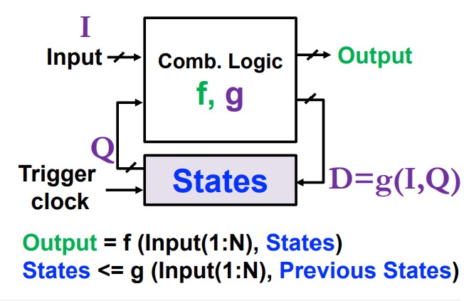
Clock
- Ring Oscillator
- LC oscilator
- Crystal Oscillator
State and FSM
States contain all needed infomation. could be redundant.
Finite State Machine(FSM) The number of input, output and states are finite.
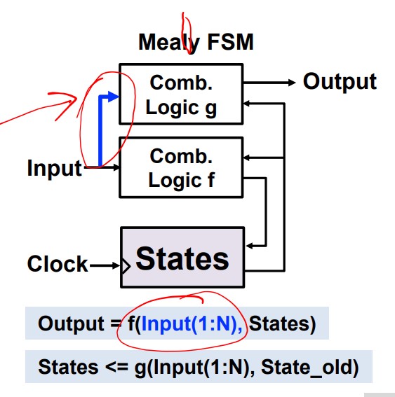
Mealy FSM:
Moore FSM:
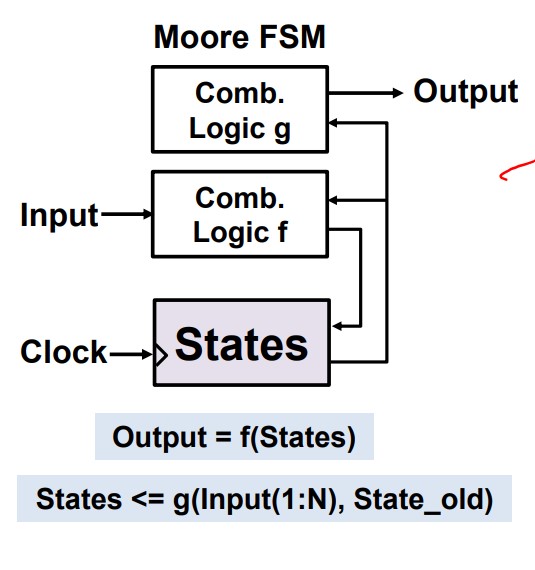
We describe the FSM by State Transition Table or State Diagram.
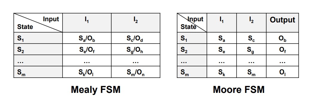
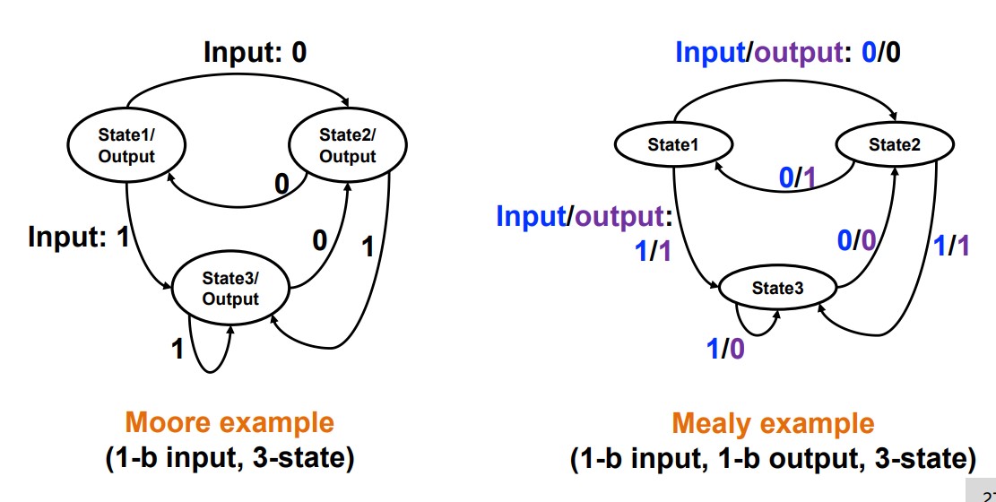
Remember: Moore is less.
Latch
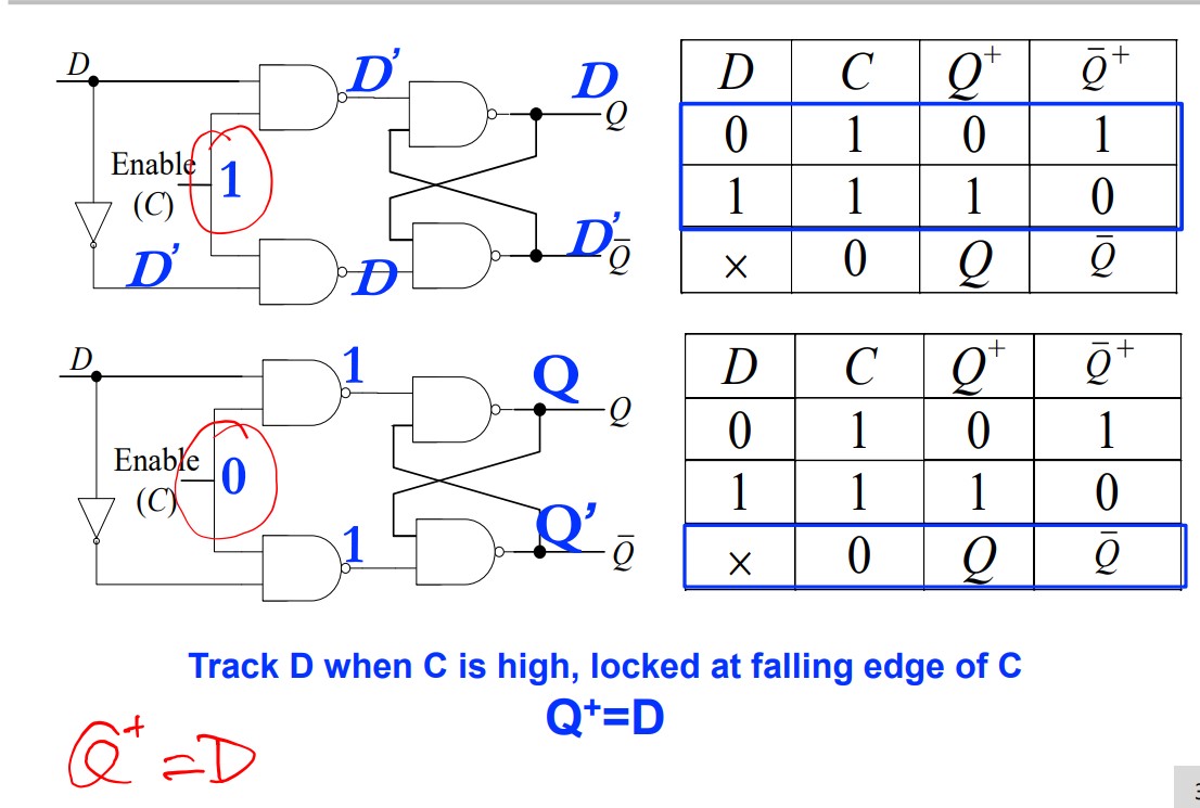
Watch the input at the duration clock enables.
Examples
SR latch
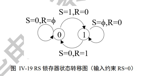
A gated version:
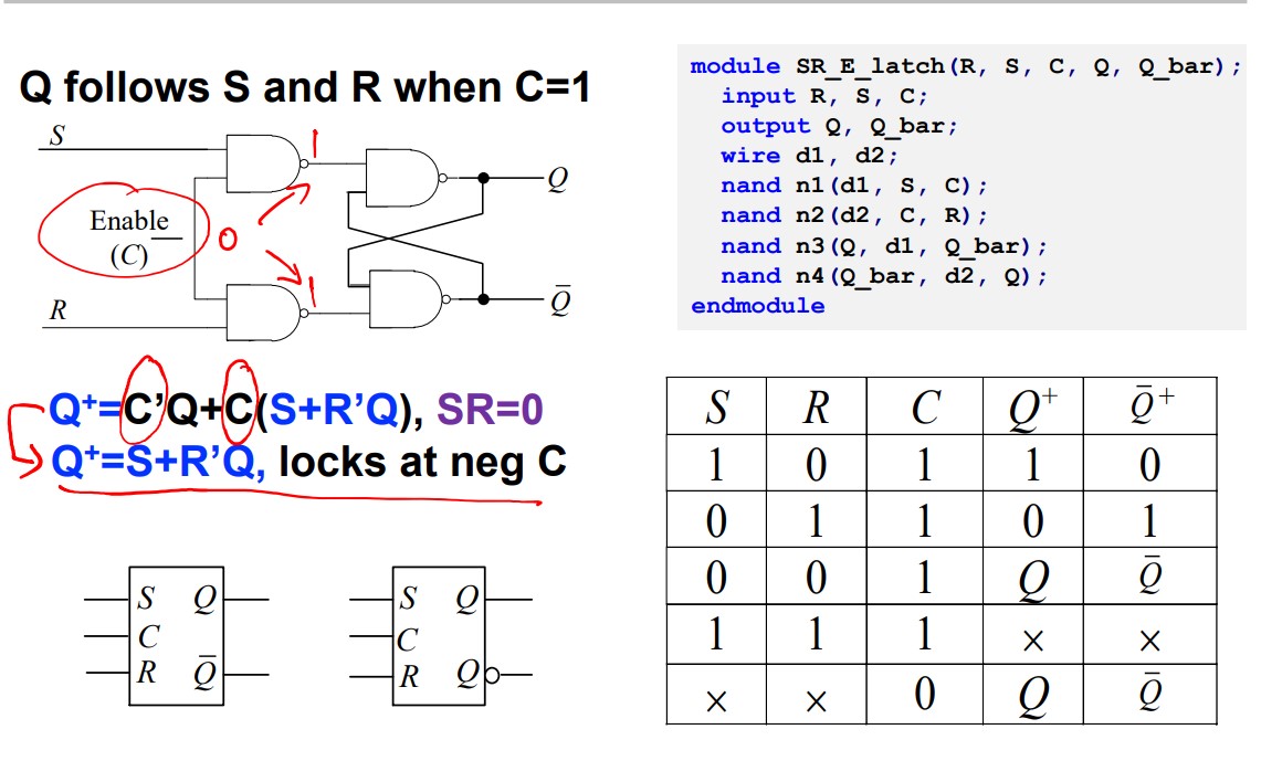
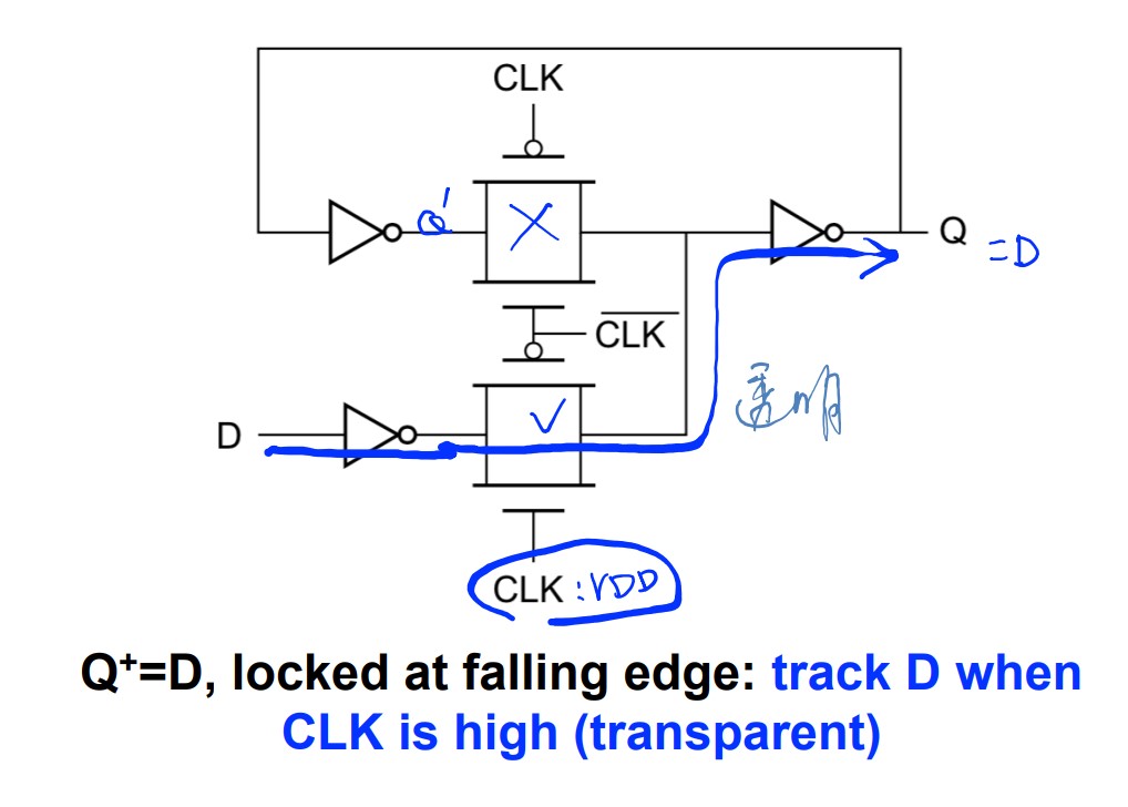
D latch
Transimission Gate version
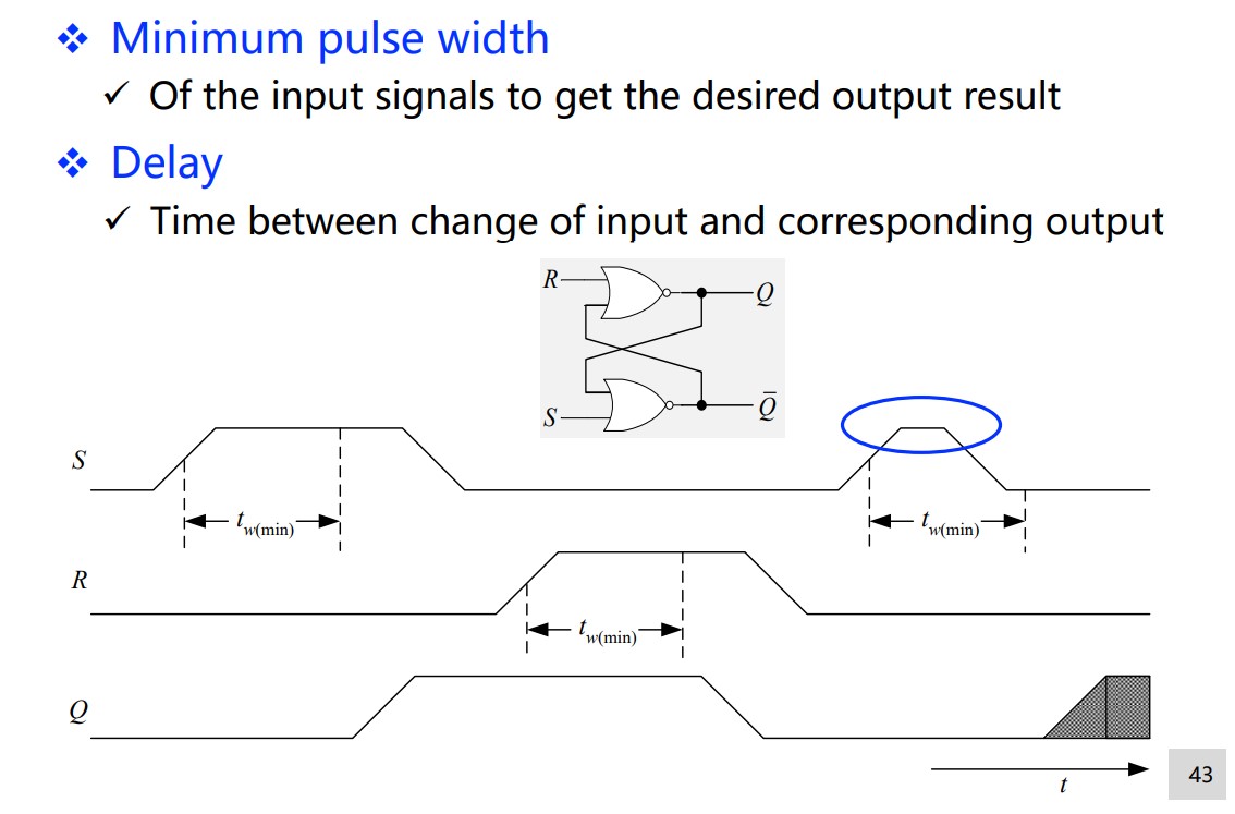
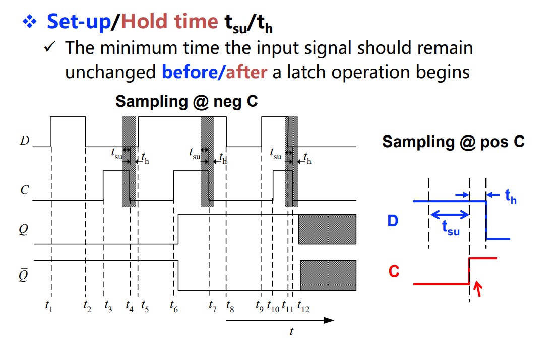
Timing parameters
Flip-Flop
Watch the input only at the moment when clock signal rises or falls.
Examples
D Flip-flop(DFF)
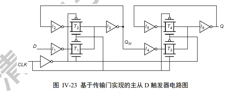
2 D latches in series with opposite clock.
Use the delay to help us
The delay of NOT gate at the bottom enables the slave to lock first and the master to unlock second when clock falls.
Also, the delay of NOT gate at the bottom makes $t_h=0$ .

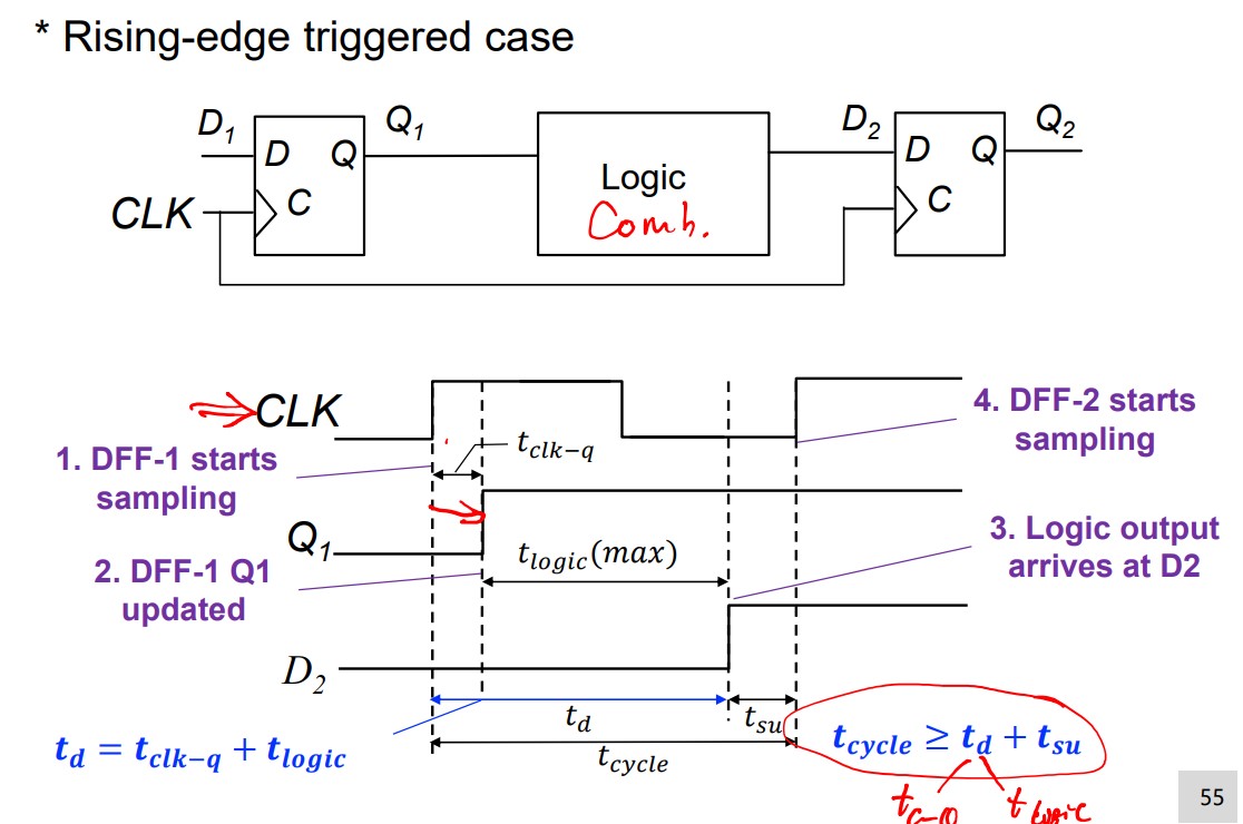
Two time constraints
Set-up time constraints: restrict the clock cycle.
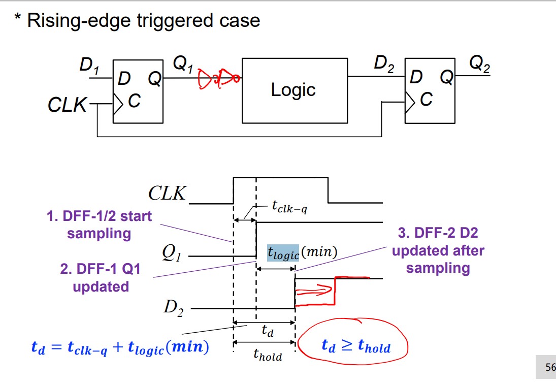
Hold time constraints: restrict the $t_d$
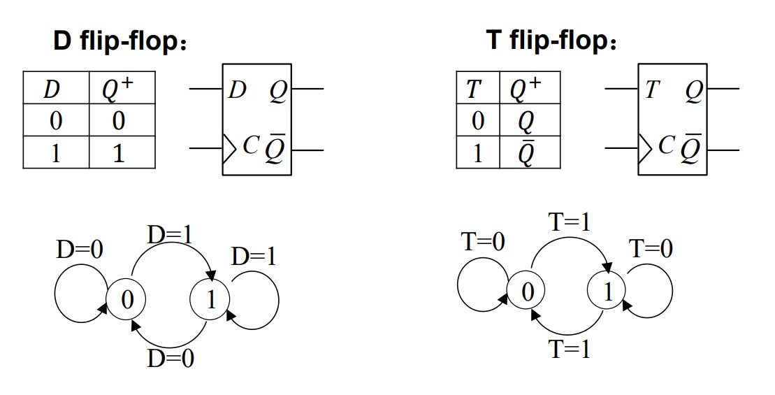
4 types of FF
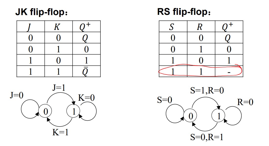
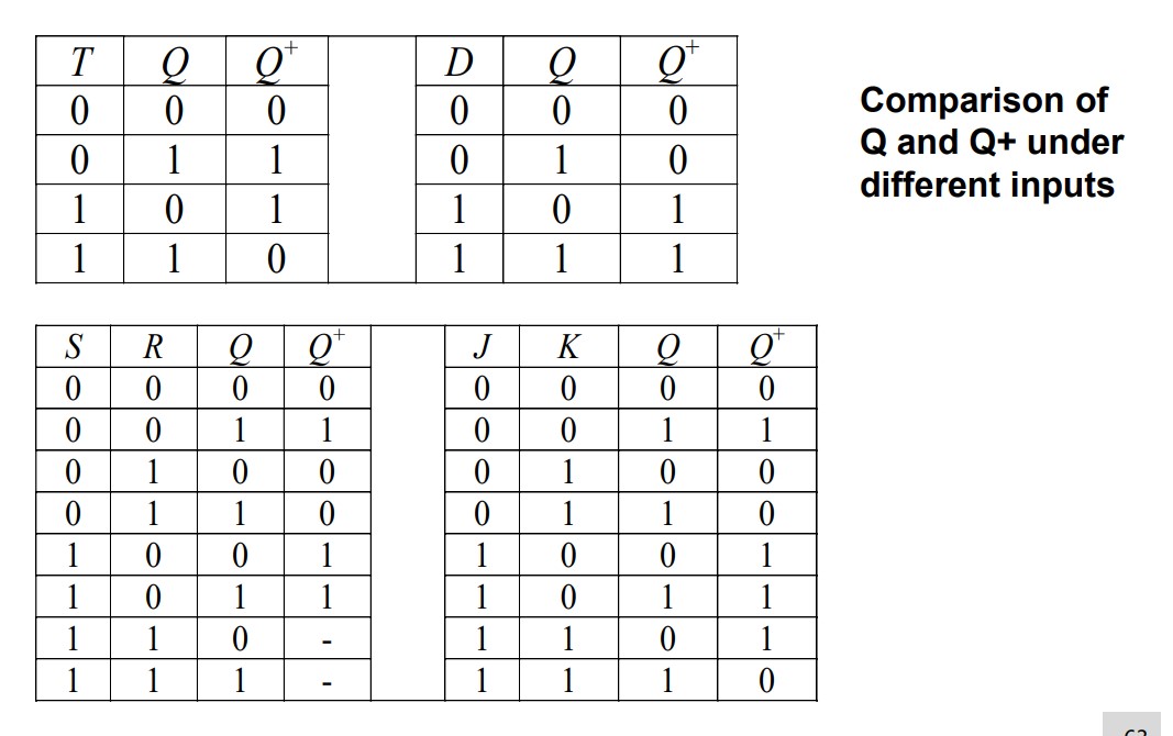
Characteristic equations
$$ Q^+=D\\ Q^+=T\overline Q + \overline{T}Q\\ Q^+=S+\overline{R}Q\\ Q^+=J\overline{Q}+\overline{K}Q $$Problems
Can $t_h$ be negative?
How to convert FF?
https://blog.csdn.net/qq_43975016/article/details/121193168
Analyzing Sequential Logic
Function Analysis
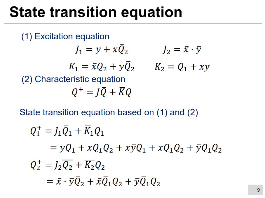
State Transistion Table
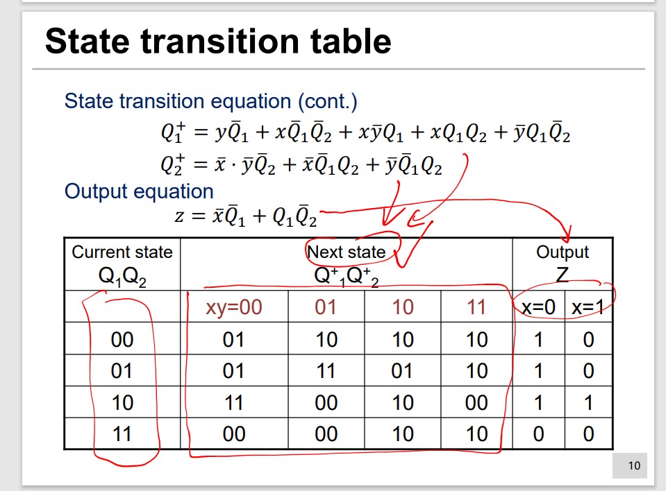
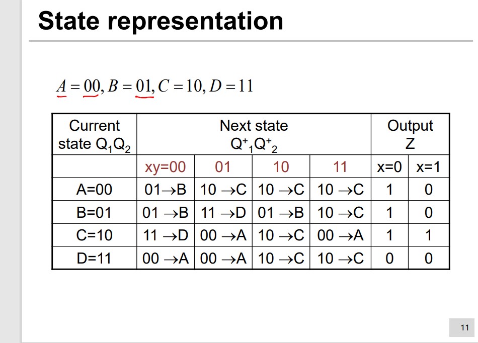
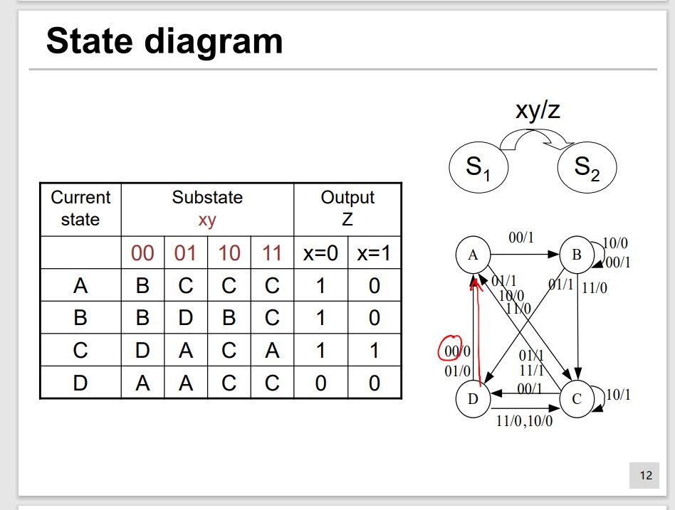
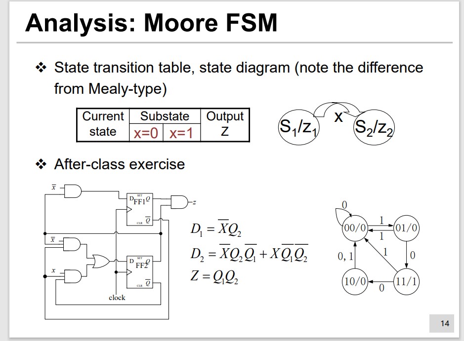
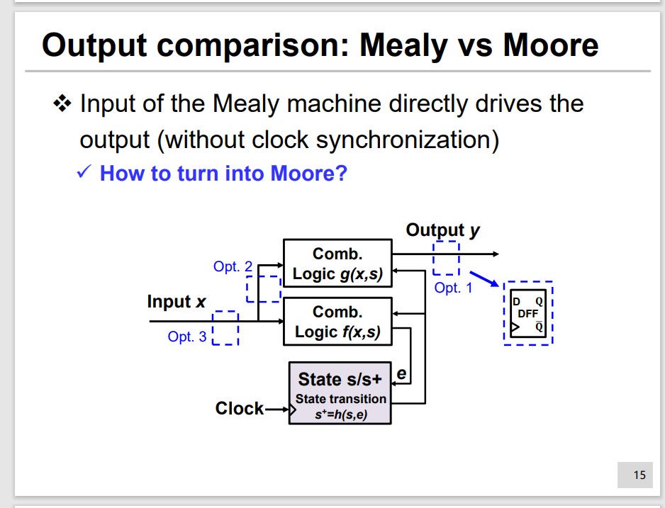
Opt.2 is different and needed to be thought carefully. The x and s in $g(x, s)$ may not be caused by same x.
Time Constraint
Designing Sequential Logic
Step 1 Determine the input, output and state
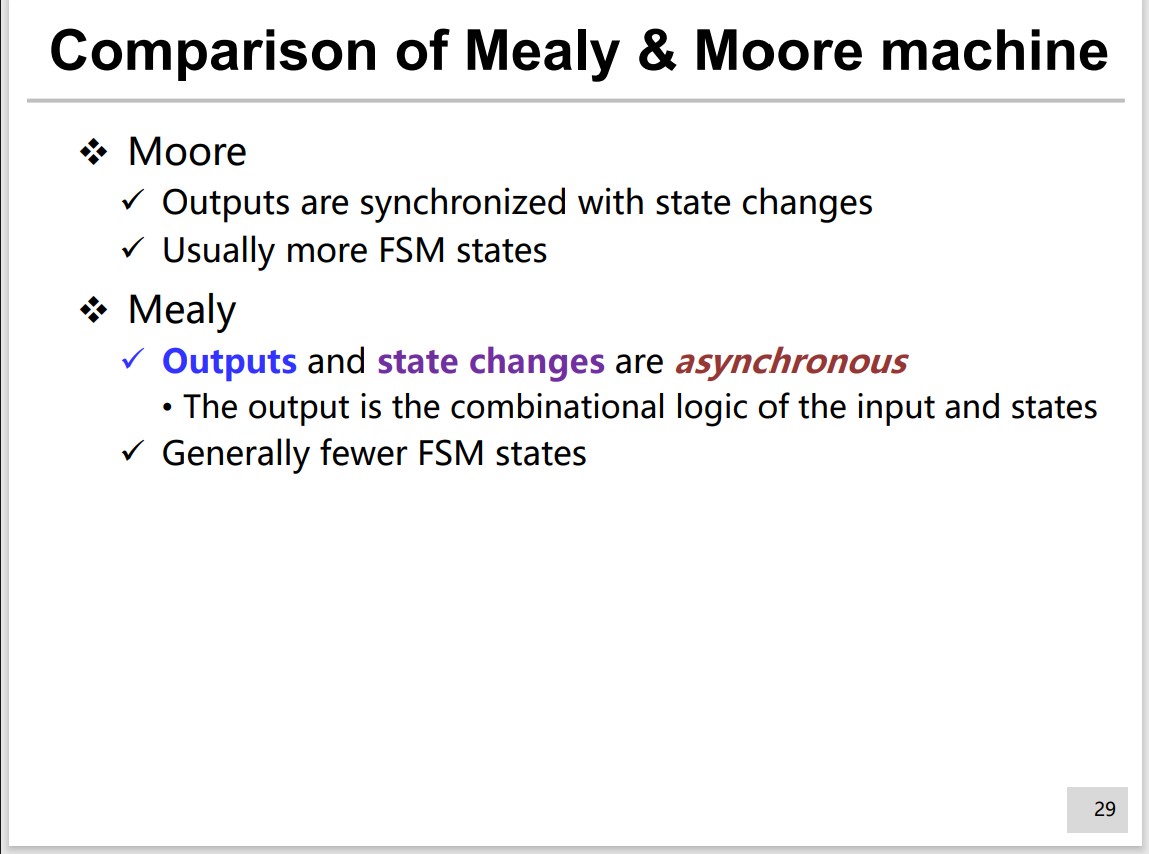
Here, Moore is more in FSM states.
Step 2 State simplification
2 methods: row matching & implication chart
row matching: $P\equiv Q$ iff. outputs and next states are same.
We can use implication table to optimize the row matching method.
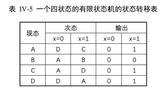
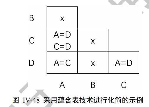
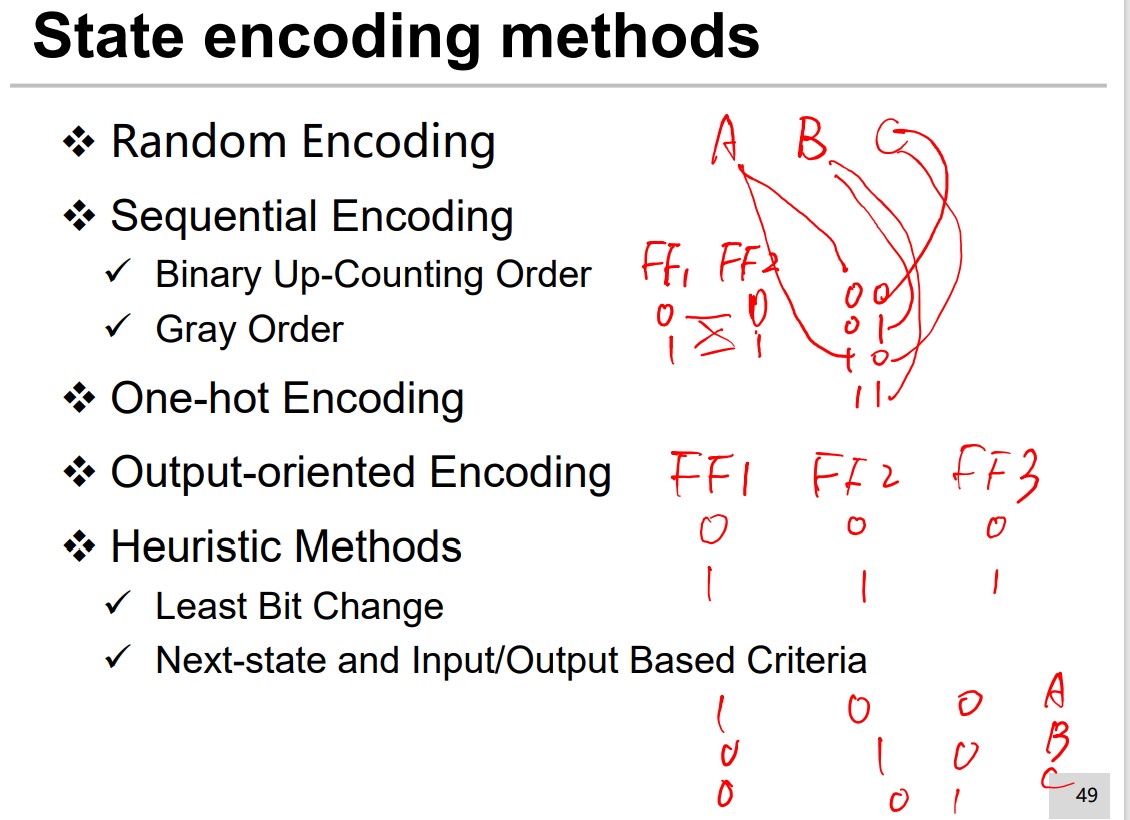
Step 3 State allocation/representation
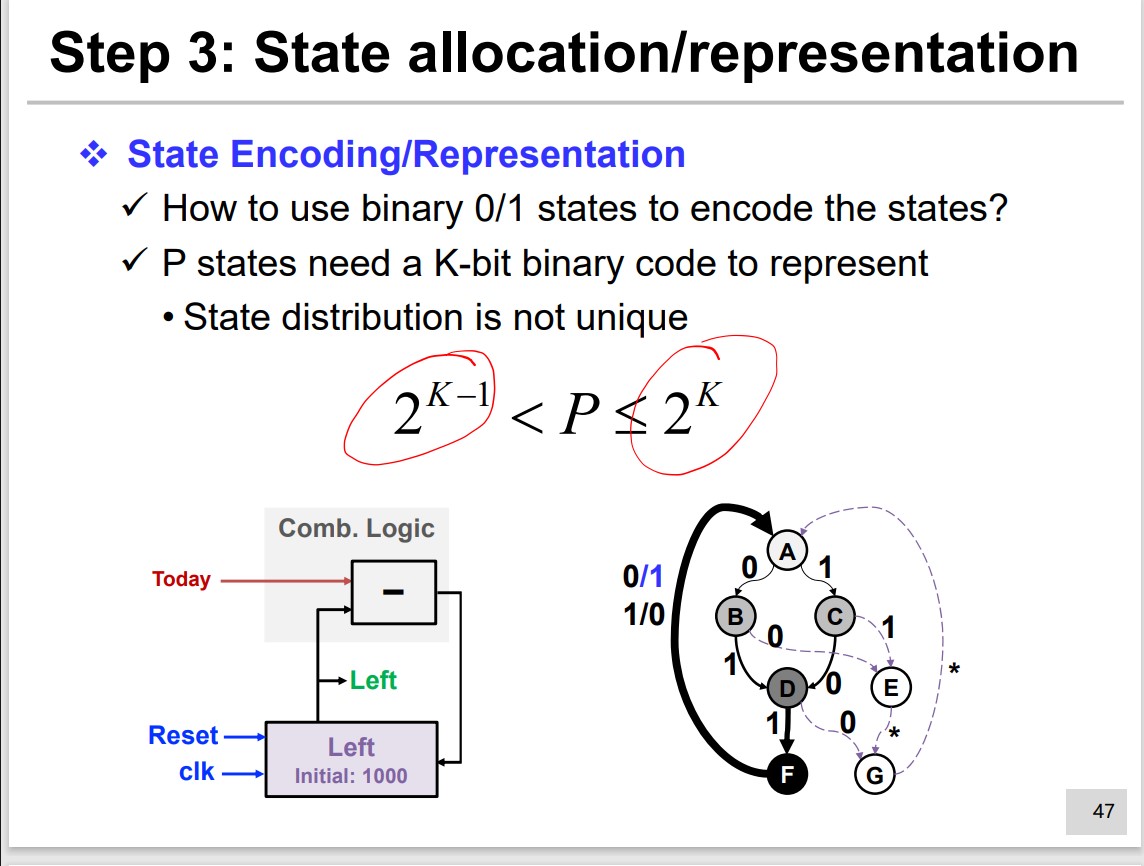
Many methods:
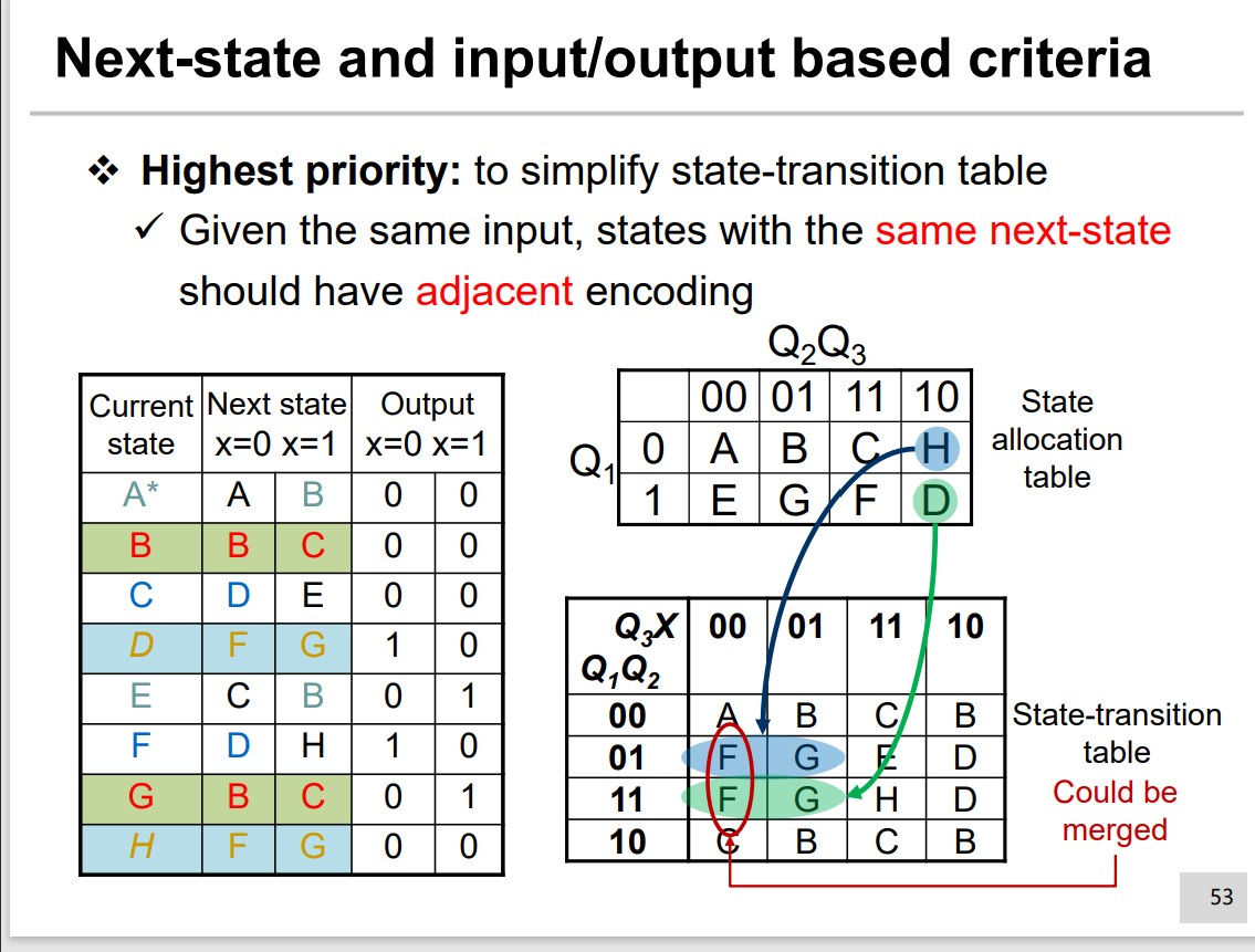
Next state and input/output based criteria
Highest Priority:
Same input and same next state should be encoded adjacently.
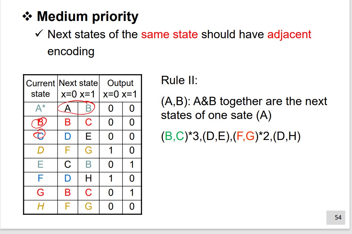
Medium Priority:
Next states of the same state should have adjacent
encoding.
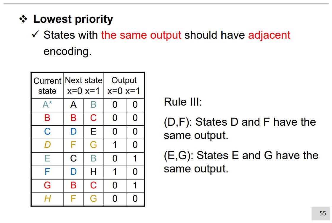
Lowest Priority:
States with the same output should have adjacent
encoding.
Step 5 Get Excitation and Output Equations
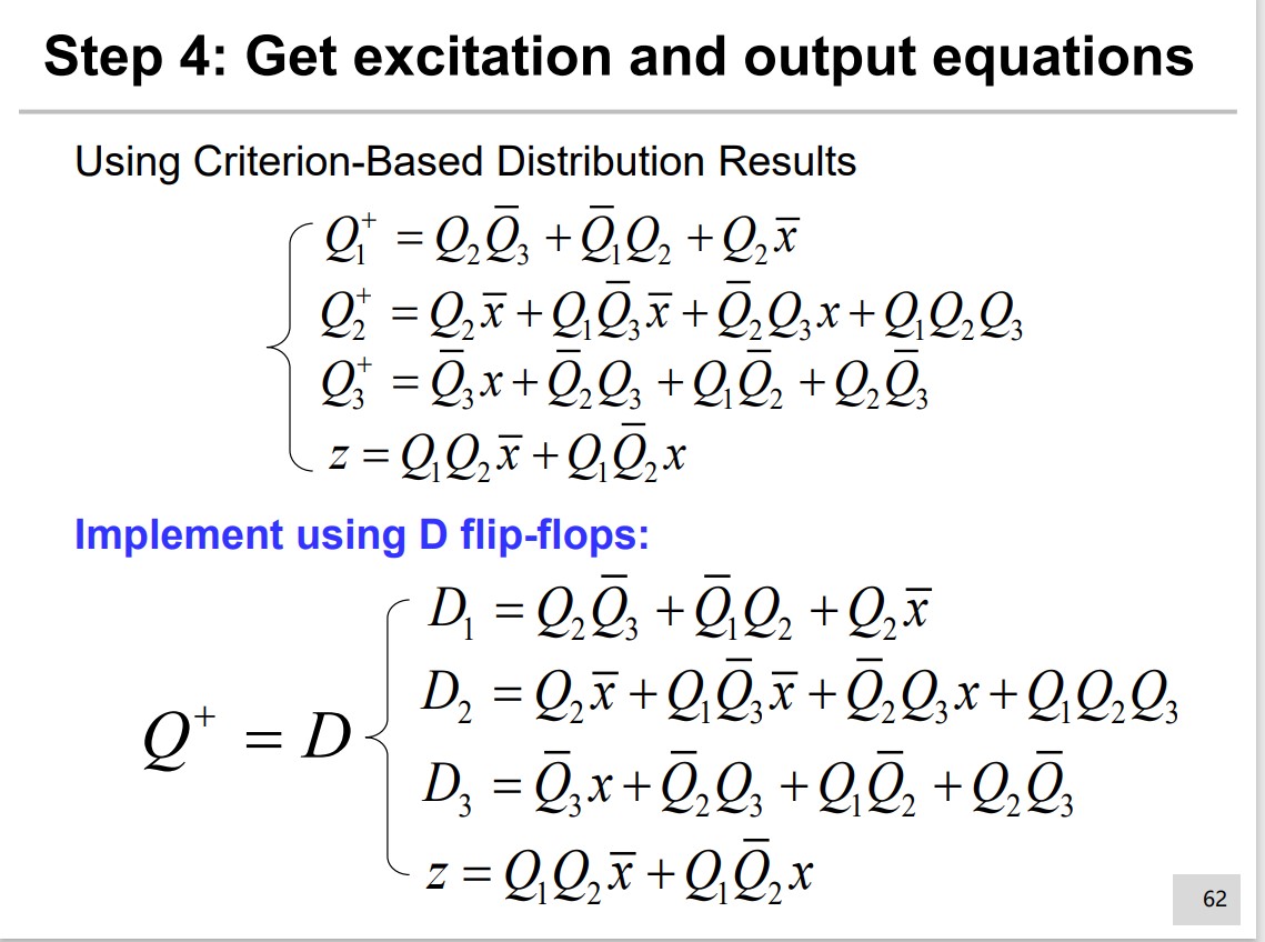
Step 6 Draw Logic Circuit Diagram
Typical Sequential Logic Circuits
Register & Counter
Register
Shift register. Serial/Parallel Input, Serial/Parallel Output.
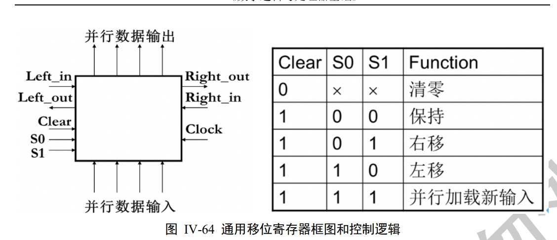
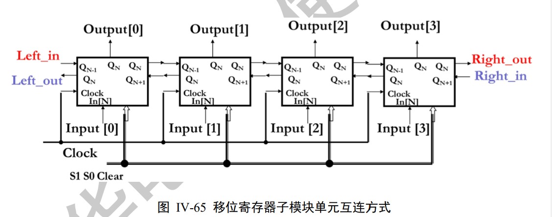
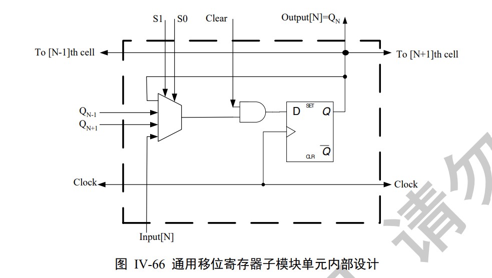
Counter
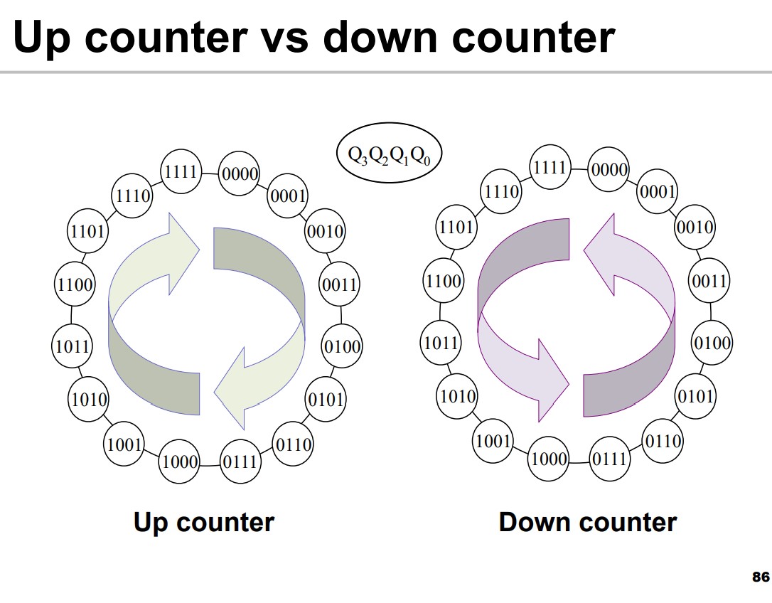
UP/Down Counter
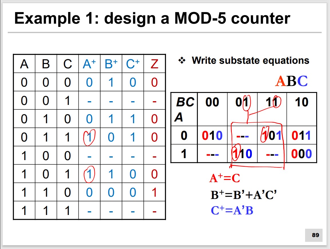
Specific-base Counter
000→010→011→101→110→000
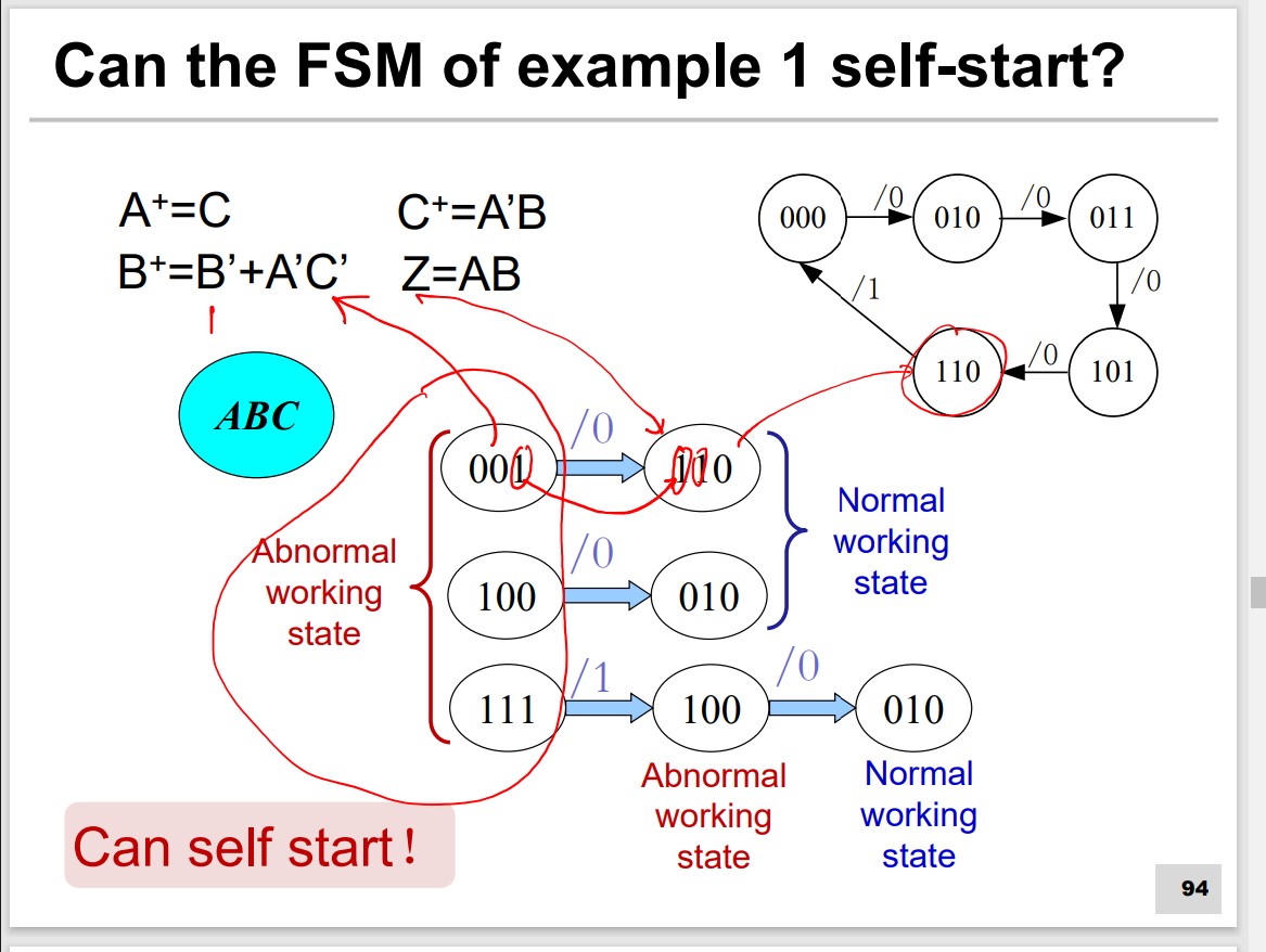
Self-Starting problem of counter
Abnormal state(001, 100, 111)
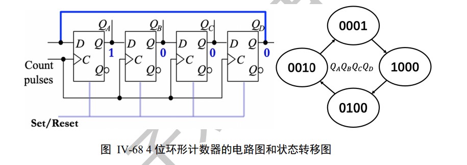
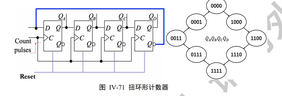
Ring counter & twisted ring counter
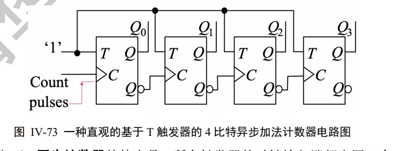
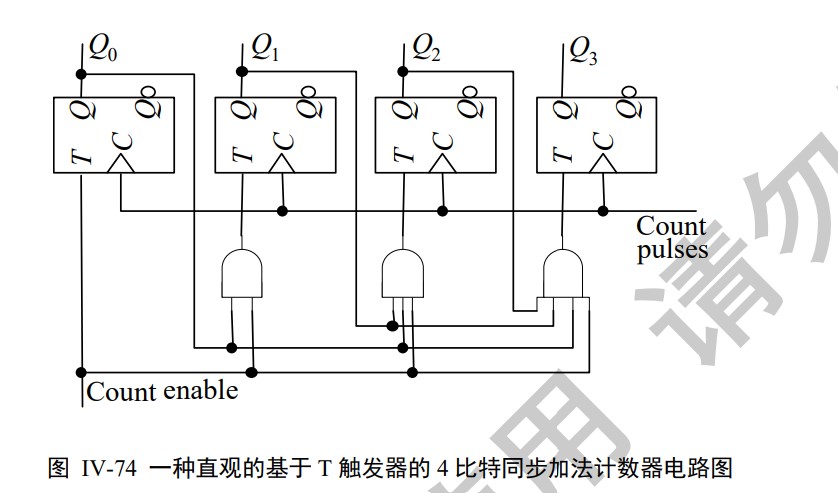
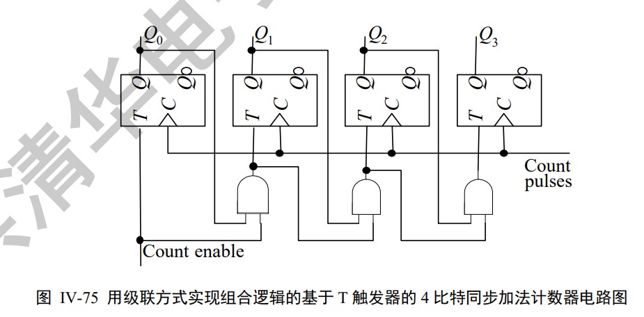
Async & snyc Counter
Instruction Set Architecture
Introduction
Implement Algorithm In Hardware
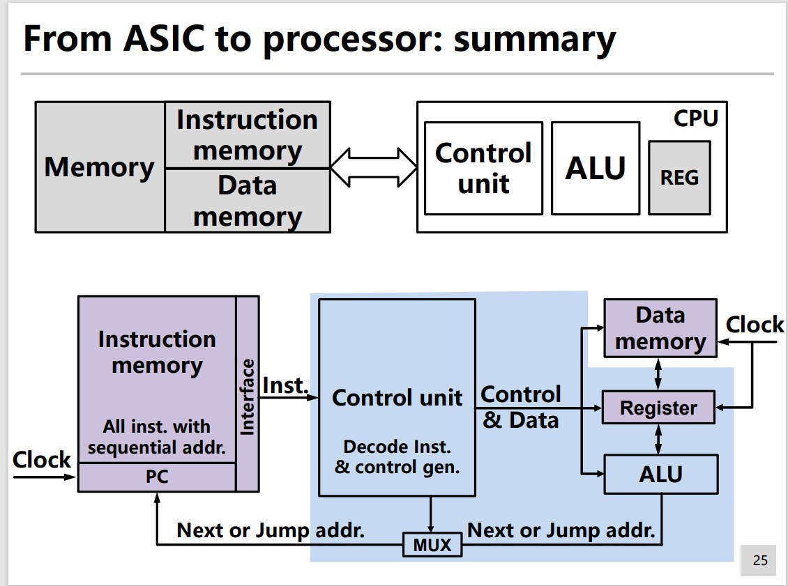
Three steps:
- Instruction fetch
- Instruction decoding
- Instruction execution & data write-back
Program Counter(PC)
Current Instruction Address
Updated Every Cycle
Arithmetic/Logic Instructions
Arithmetic Logic Unit(ALU)
REG to REG, NOT Directly access data memory
Branch/Jump Instructions
Branch After Comparison
Jump Directly
Load/Store Instructions
Load Data: data memory to REG
Store Data: REG to data memory
General Purpose Processore Structure
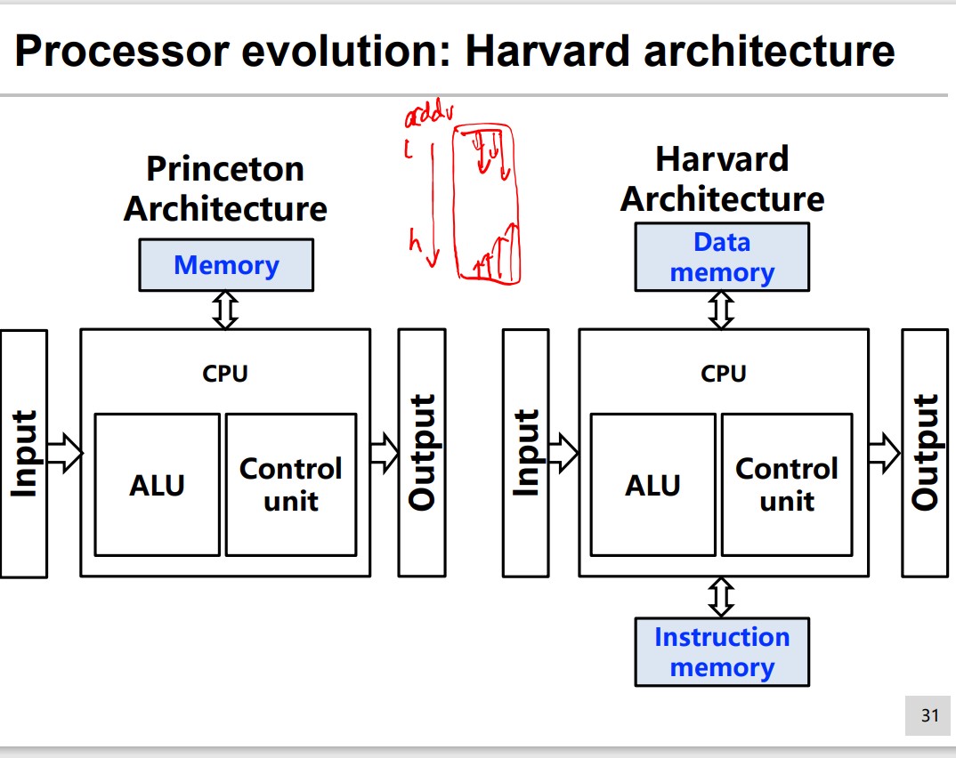
Turing Machine
2 Turing Machine Models:
- Princeton architecture
- Harvard architecture
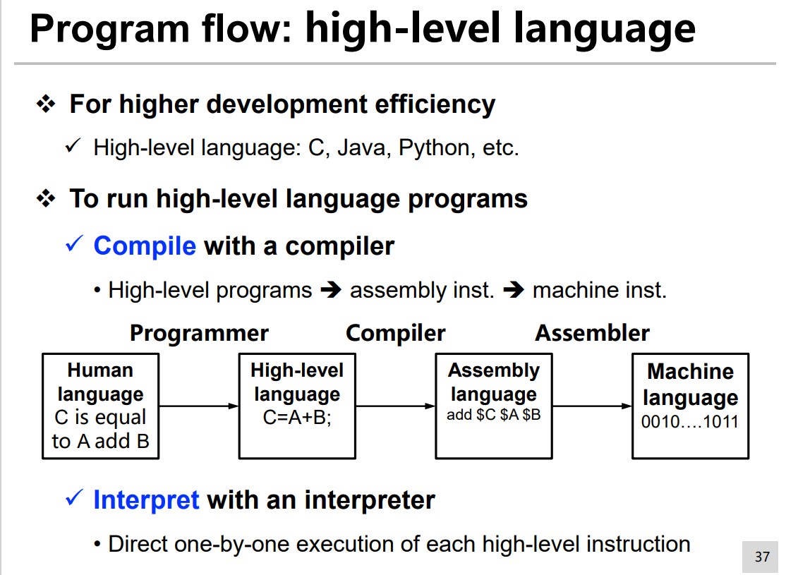
Program FLow
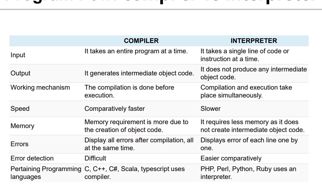
Instruction Set Design
Instruction set is the bridge between software & generall-purpose (GP) CPU.
Performance Evaluate
$$ \text{Performance} = \frac{1}{\text{Execution Time}} $$Task Execution Time By CPU:
$$ \text{Total Time} = \text{Waiting for I/O} + \text{Execution Time}\\ \text{Execution Time} = \text{Cycle }\# \times \text{Clock Cycle }T = \frac{\text{Cycle }\# }{\text{Clock }f} $$ $$ \text{Cycle } \# = \text{Progream Instruction }\# \times \text{Average Cycle } \# \text{ for one inst.} $$Average Cycle # for one instruction is also known as the cycle per instruction (CPI)
So,
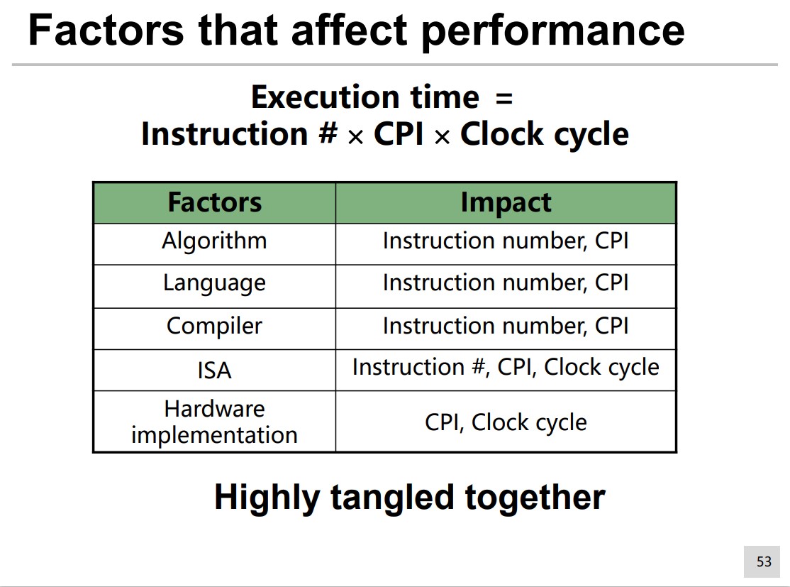
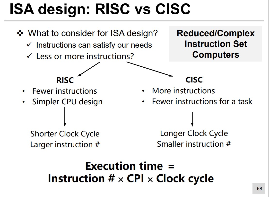
$$ \text{Execution Time} = \text{Instruction }\# \times \text{CPI} \times \text{Clock Cycle } $$CPI
$$ \text{CPI} = \sum_{i = 1}^n \text{CPI}_i \times \text{P}_i $$Where $\text{P}_i$ is the i-th instruction occurrence frequency, and $\text{CPI}_i$ is the clock cycle # of the i-th instruction.
Factors that affect Performance
- Instruction #
- ISA, regardless of its specific implementation
- Compiler
- CPI
- Memory System and Processor Architecture
- The Instruction Composition In the Program
- Compiler
- Clock Cycle
- Machine implementation details
- Memory System and Processor Architecture
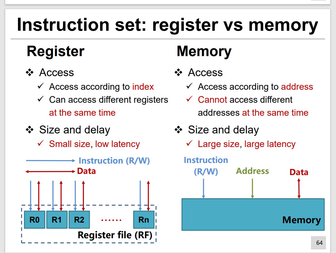
Data Access
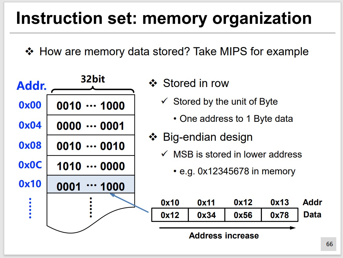
Set Design
RISC & CISC
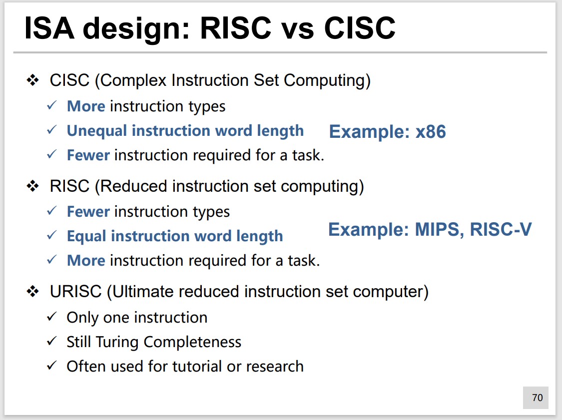
Five Questions
- How to make use of 11 extra bits in arithmetic operations?
- How to use 16 bits to represent 32-bit address for branch?
- How to encode branch instruction with immediate?
- How to use 21 bits to represent 32-bit address for memory address?
- How to use 26 bits to represent 32-bit address for jump?
MIPS Instruction Set
Instruction Storage and Data Storage
32-bits instruction length, and 32 general-purpose registers.
First 6 bits are opcode.
Register
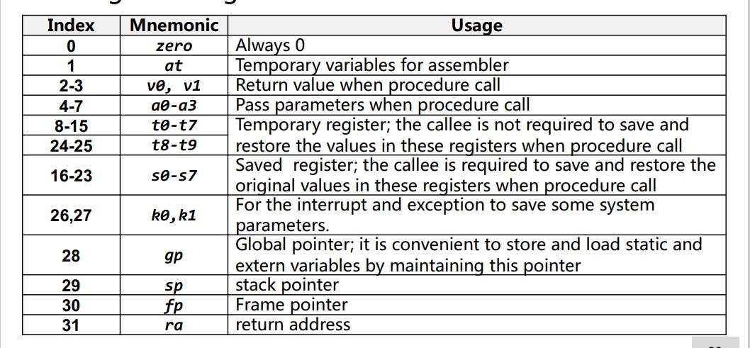
the register index is limited to 5 bits.
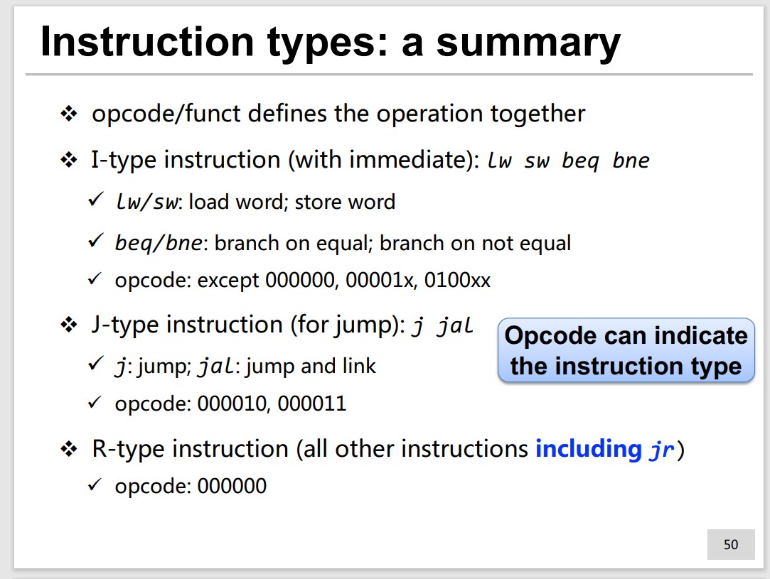
Instruction Type(R, I, J)
Type: R
Field Division and detailed definition
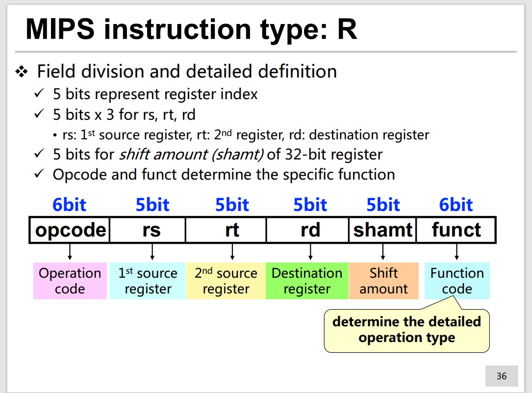
Q1: Can we make use of the extra 11 bits?
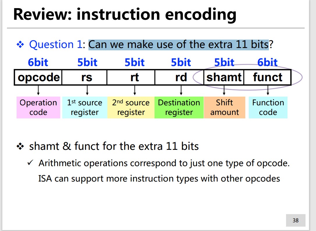
Type: I
It’s immediate.
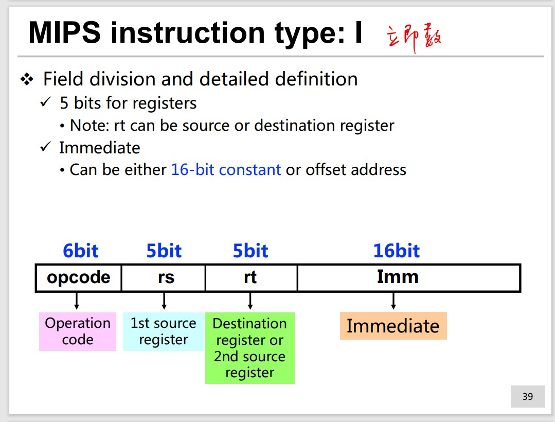
2 cases:
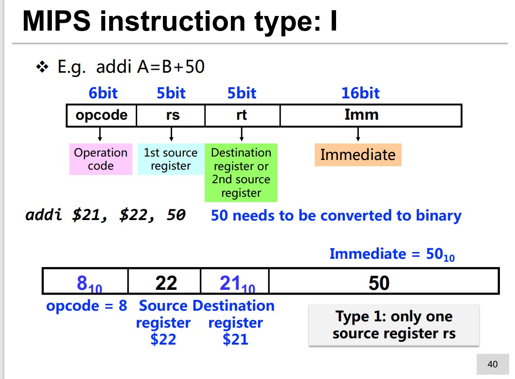
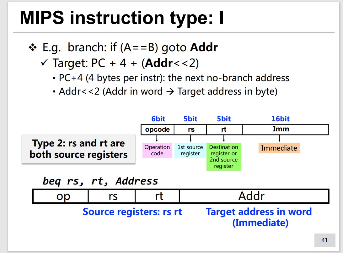
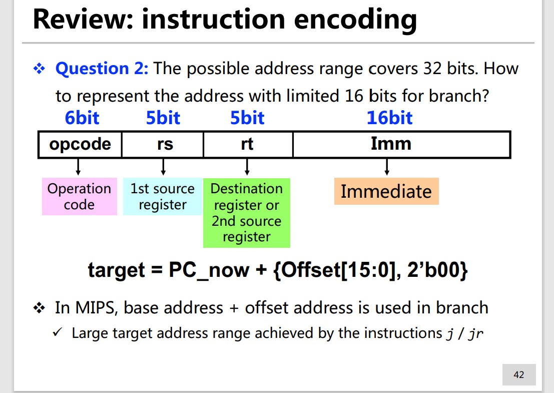
Q2:The possible address range covers 32 bits. How to represent the address with limited 16 bits for branch?
base + offset
Q3: How to encode the branch with immediate?
No direct instructions for this.
We use compare instruction and branch instruction to achieve this.
Q4: The possible address range covers 32 bits. How to represent the address with limited 21 bits for memory access?
base + offset
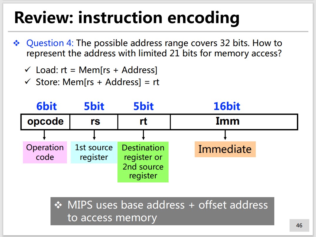
Type: J
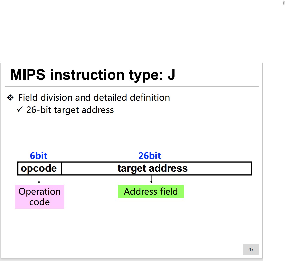
Q5: The possible address range covers 32 bits. How to represent
the address with limited 26 bits for jump?
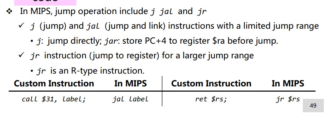
3 types of jump operation: j, jal and jr.
Summary
Addressing mode
5 modes:
- Register addressing
- Immediate addressing
- Base (base-offset) addressing
- PC-related addressing
- Pseudo-direct addressing
Register addressing
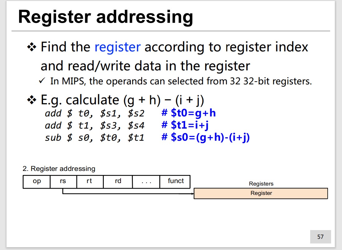
Immediate addressing
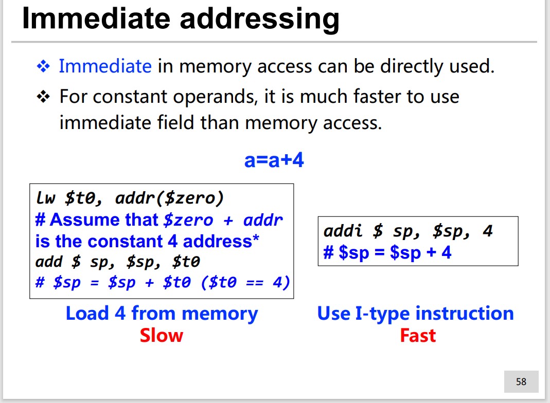
How to load a 32-bit constant to $s0?
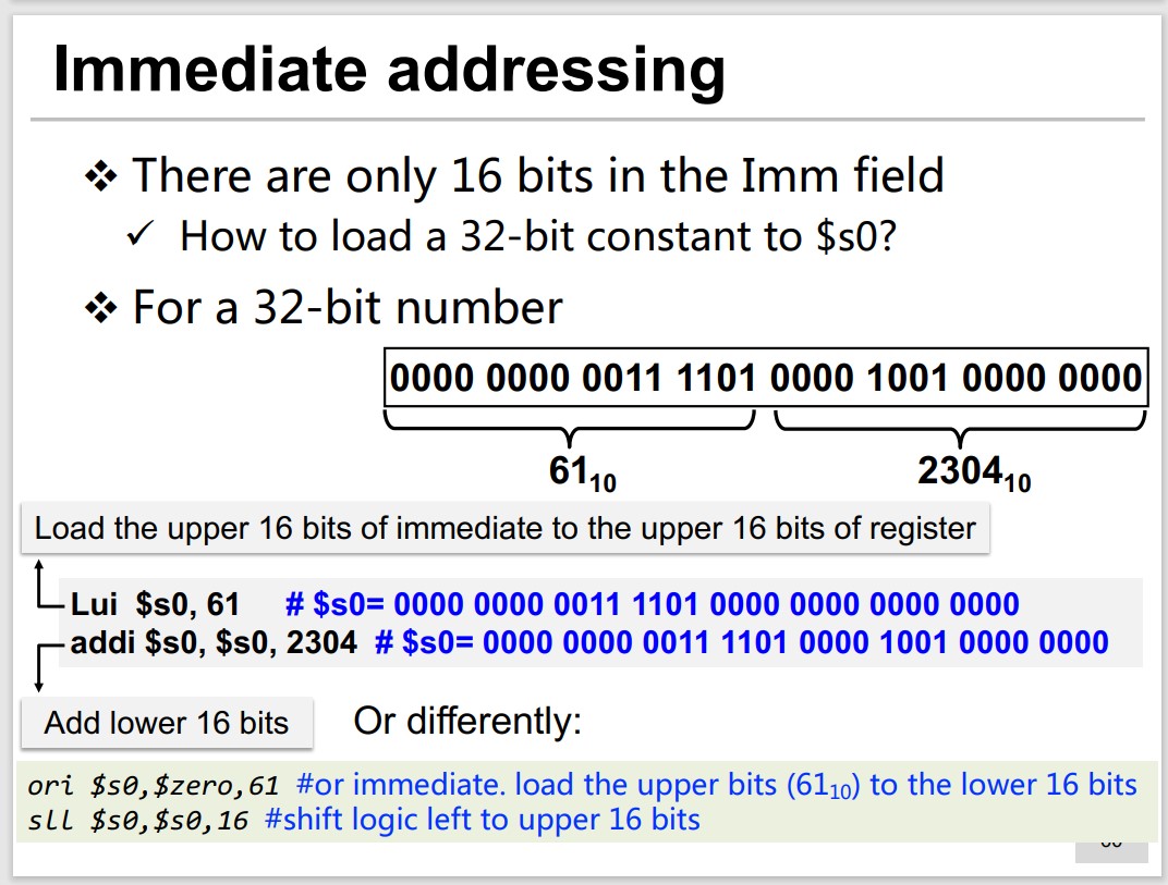
Base-offset addressing
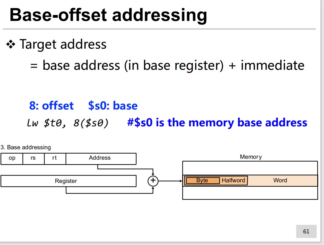
PC-related addressing
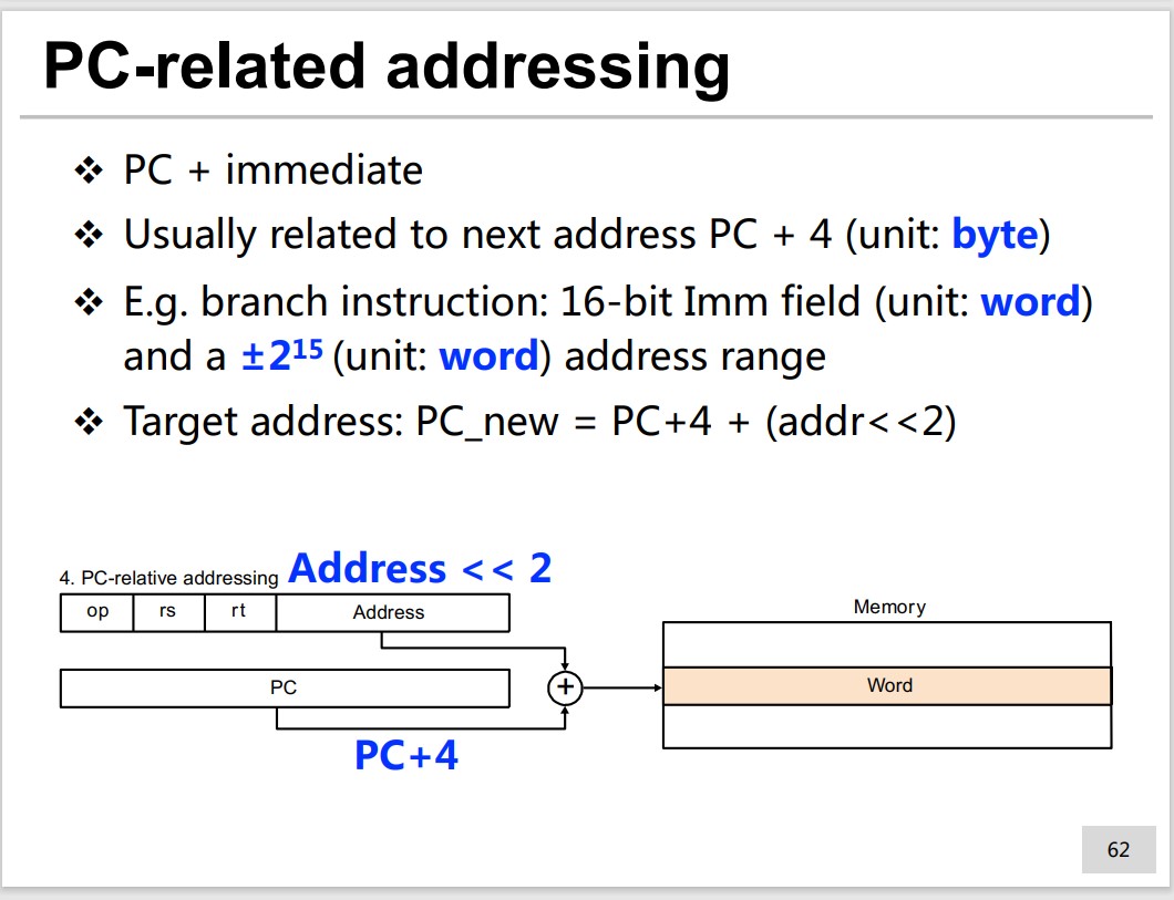
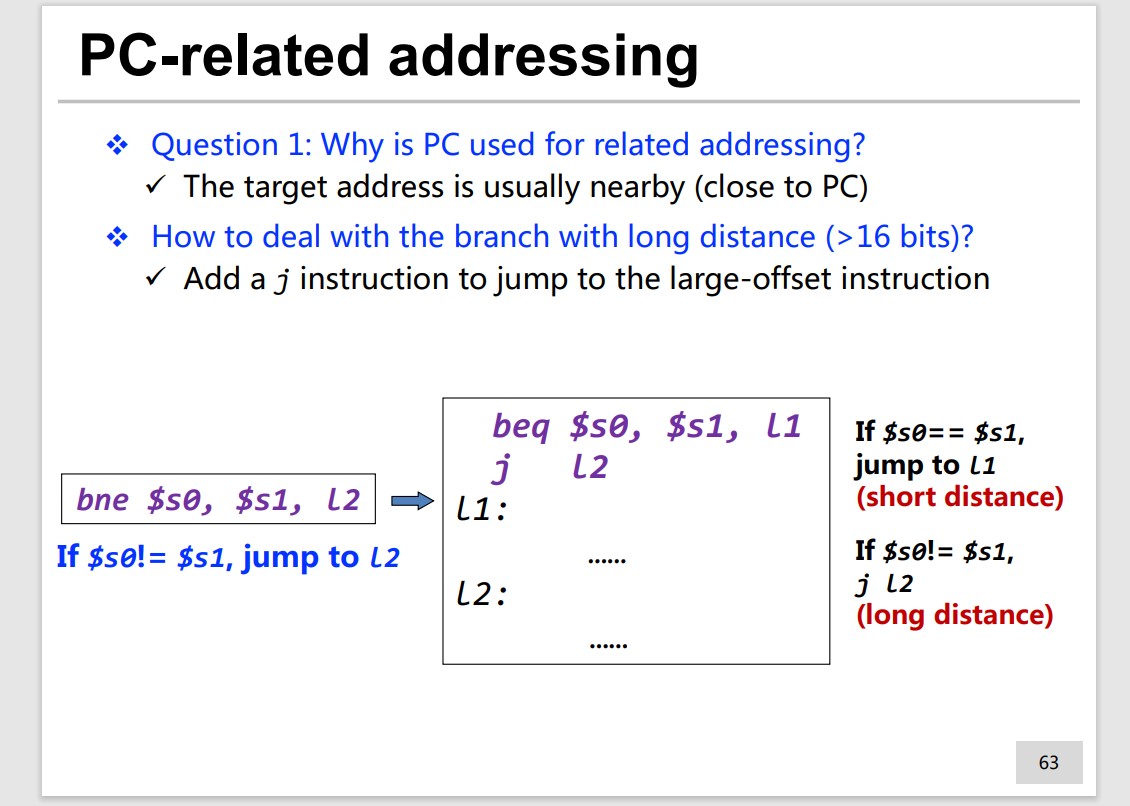
Pseudo-direct addressing
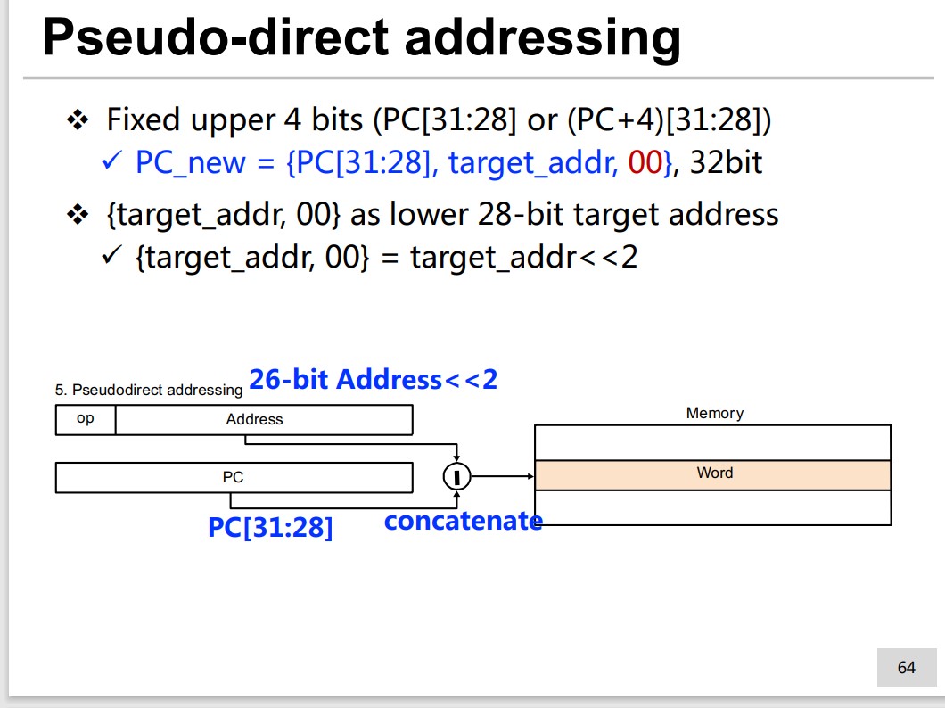
It is faster because no add operation needed, comparing to PC_new = {PC_old + address << 2}.
Summary
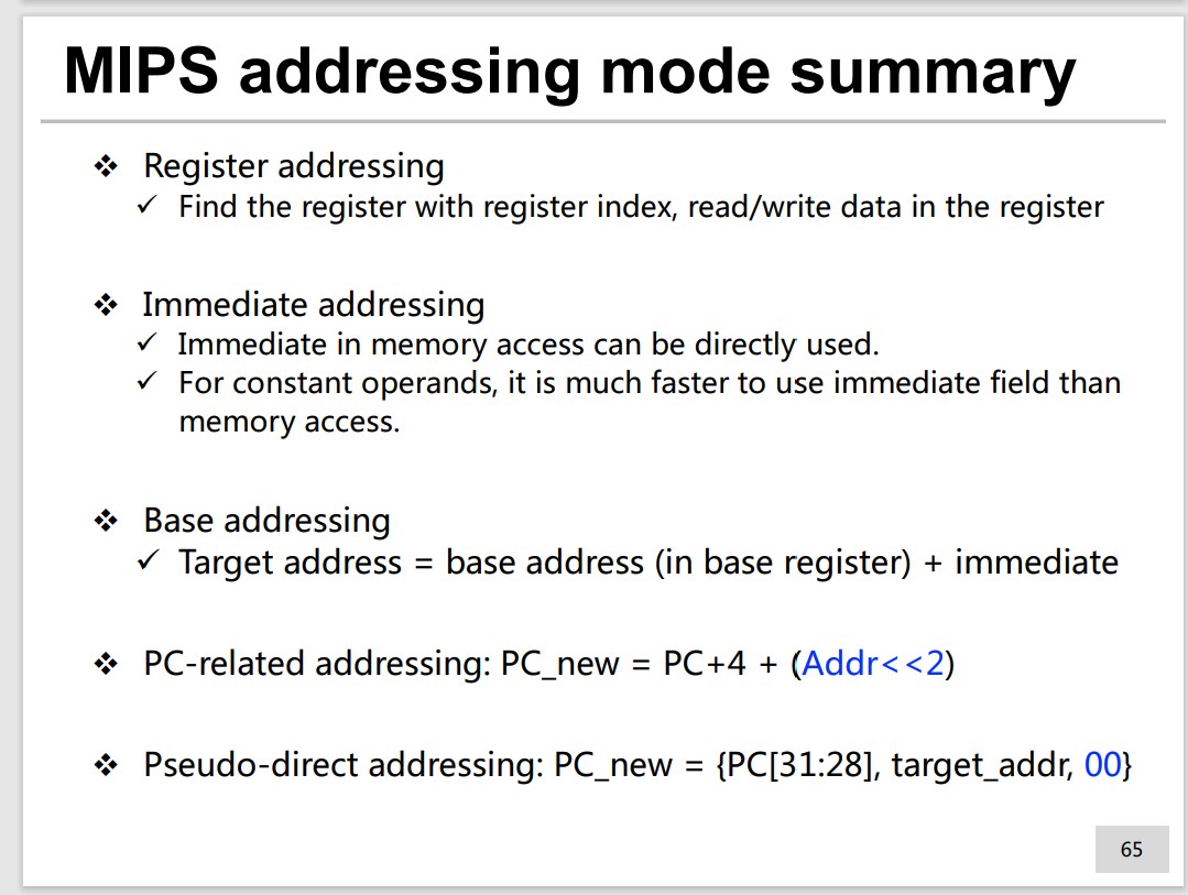
Instruciton System
Arithmetic
Add add $t0, $ t1, $t2 #$ t0= $t1+$ t2
Add immediate addi $t2, $ t3, 5 # $t2=$ t3+5
Subtract sub $t2,$ t3, $t4 #$ t2= $t3-$ t4
NO subtract-an-immediate instruction! We use 2’s complement immediate in the addi.
Logic
1 | and {% raw %} $t0, $ {% endraw %}t1, {% raw %} $t2</span><br><span class="line">or $ {% endraw %}t0, {% raw %} $t1, $ {% endraw %}t2 |
No NOT instruction. We set $t1` or `$ t2 to 0 and use NOR.
With immediate:
1 | andi {% raw %} $t0, $ {% endraw %}t1, 10 |
Shift
Immediate-amount shift:
1 | sll {% raw %} $t0, $ {% endraw %}t1, 10 |
Register-amonut shift:
1 | sllv {% raw %} $t0, $ {% endraw %}t1, {% raw %} $t3</span><br><span class="line"># $ {% endraw %}t0 = {% raw %} $t1 << ($ {% endraw %}t3%32), logical |
Compare instruction
1 | slt {% raw %} $t1, $ {% endraw %}t2, {% raw %} $t3</span><br><span class="line"># if ($ {% endraw %}t2 < {% raw %} $t3) $ {% endraw %}t1=1; |
With immediate:
1 | slti {% raw %} $t1, $ {% endraw %}t2, 10 |
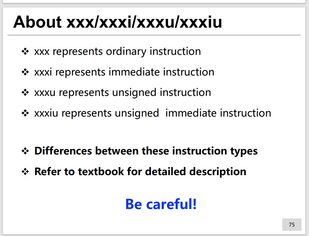
About i, u, iu
Load/Store Instruction
1 | lw {% raw %} $t1, 32($ {% endraw %}t2) |
Register stores base address is called base register,
Constant in the instruction is called offset.
Branch instruction
1 | beq {% raw %} $t0, $ {% endraw %}t1, target |
More than this 2 instructions.
Jump instruction
Unconditional branch
1 | j label |
Procedure Call
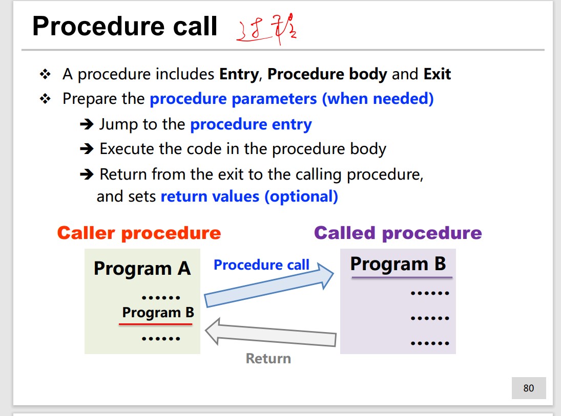
MIPS uses registers for argument and return data/address.
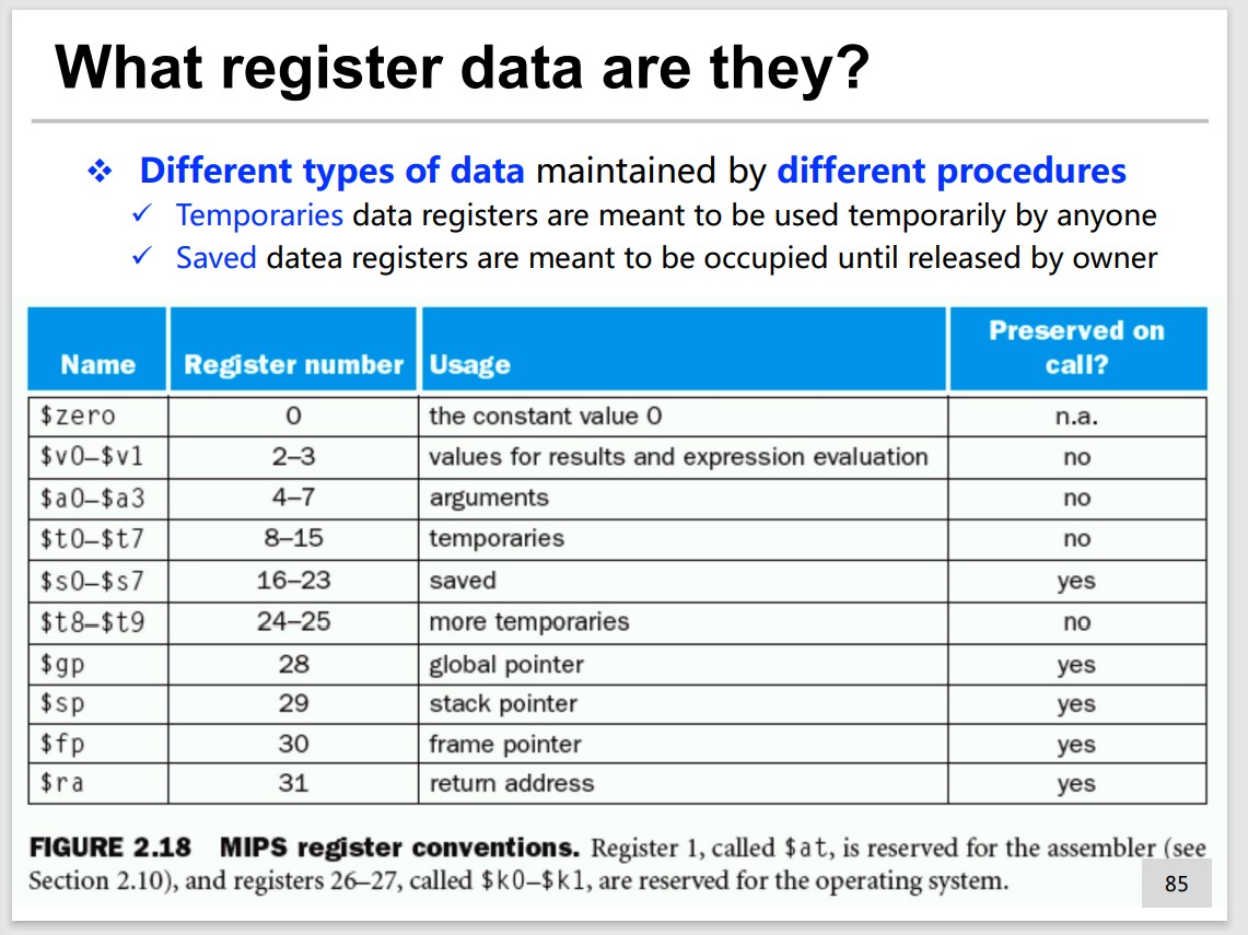
Argument registers: $a0-$ a3
Return value registers: $v0-$ v1
Retuen address register: $ra
jal Procedure #Procedure call jr $ra #Procedure return
jal and j are both J-type, but jal will store the return address.
jr is R-type, will jump to the address restored in the register, so it can jump very far.
Maintain the register data
2 types:
- Temporaries data registers
- Saved data registers
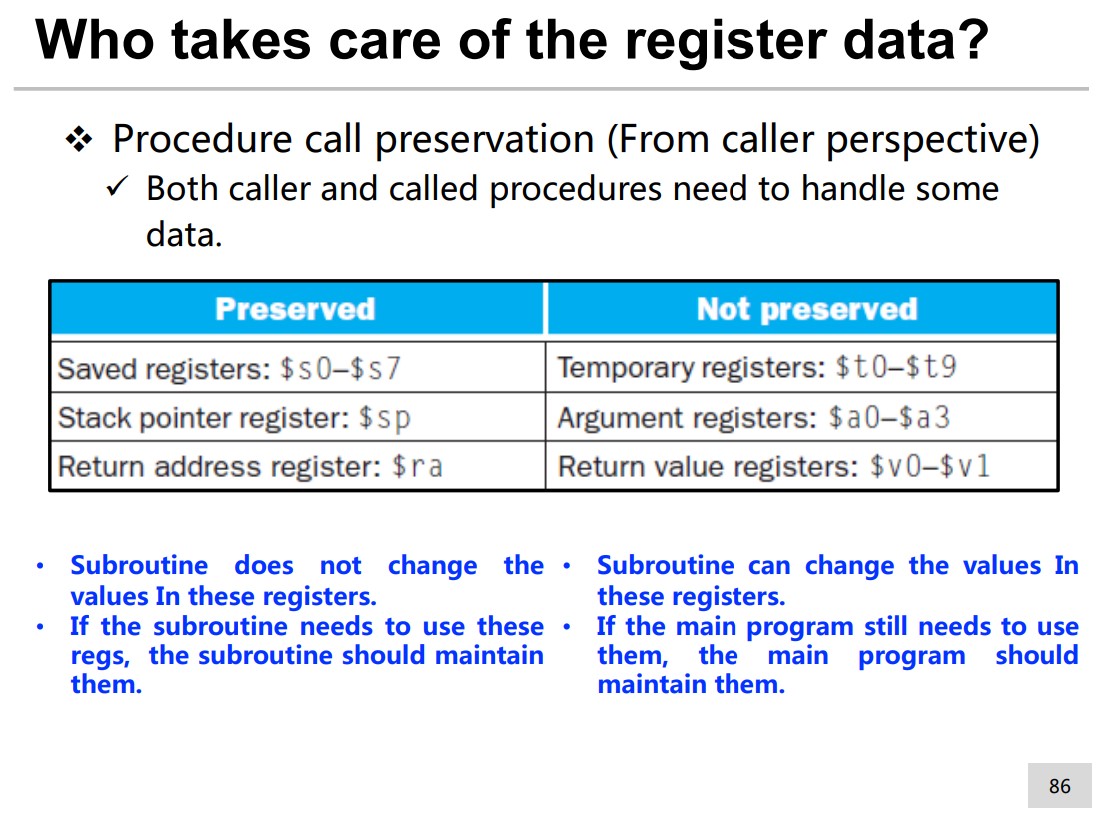
Who saves the register data?
Caller(temp) or Callee(save)
We use Stack to maintain the register data.
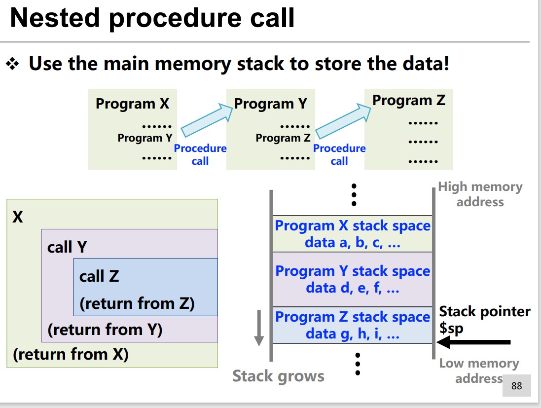
Stack Operation with $sp
e.g. push $s1, $ s2 , $s3
1 | addi {% raw %} $sp, $ {% endraw %}sp, -12 |
pop $s1, $ s2, $s3
1 | lw {% raw %} $s1, 0($ {% endraw %}sp) |
Leaf Procedures
Procedures that do not call others are called leaf procedures.
Nested Procedures
Nested(Recursive) Procedures are procedures that invoke “clones” of themselves.
e.g.
1 | int fact (int n) { |
1 | fact: |
Single-Cycle Processor
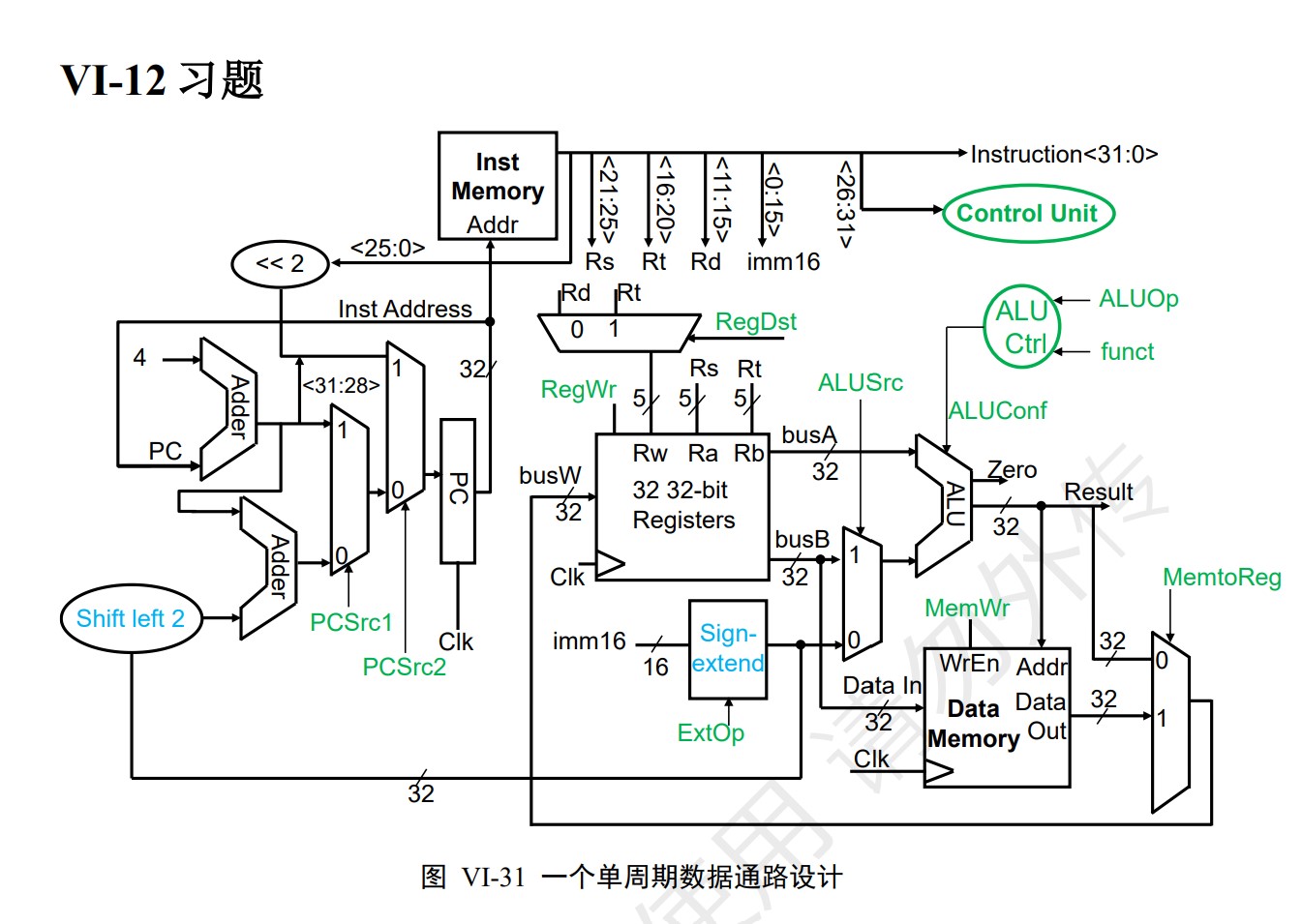
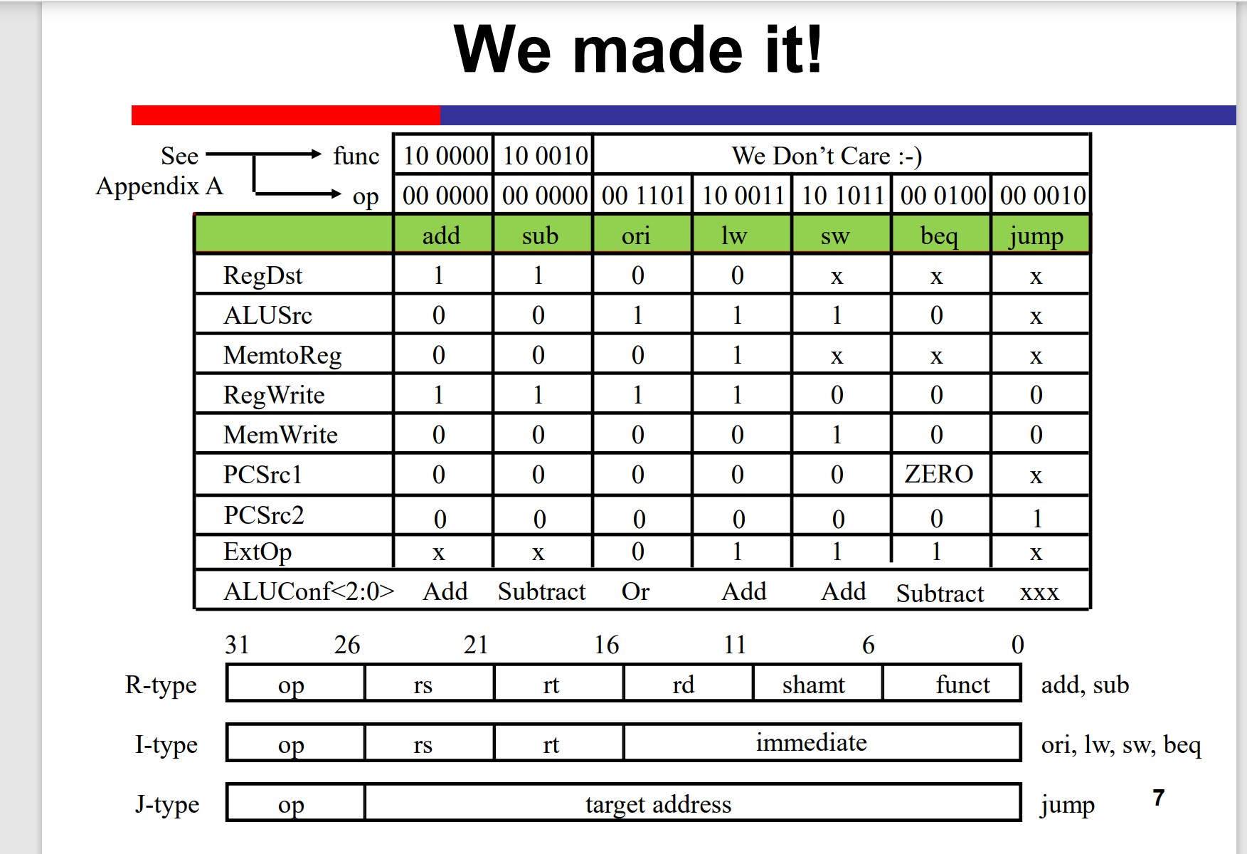
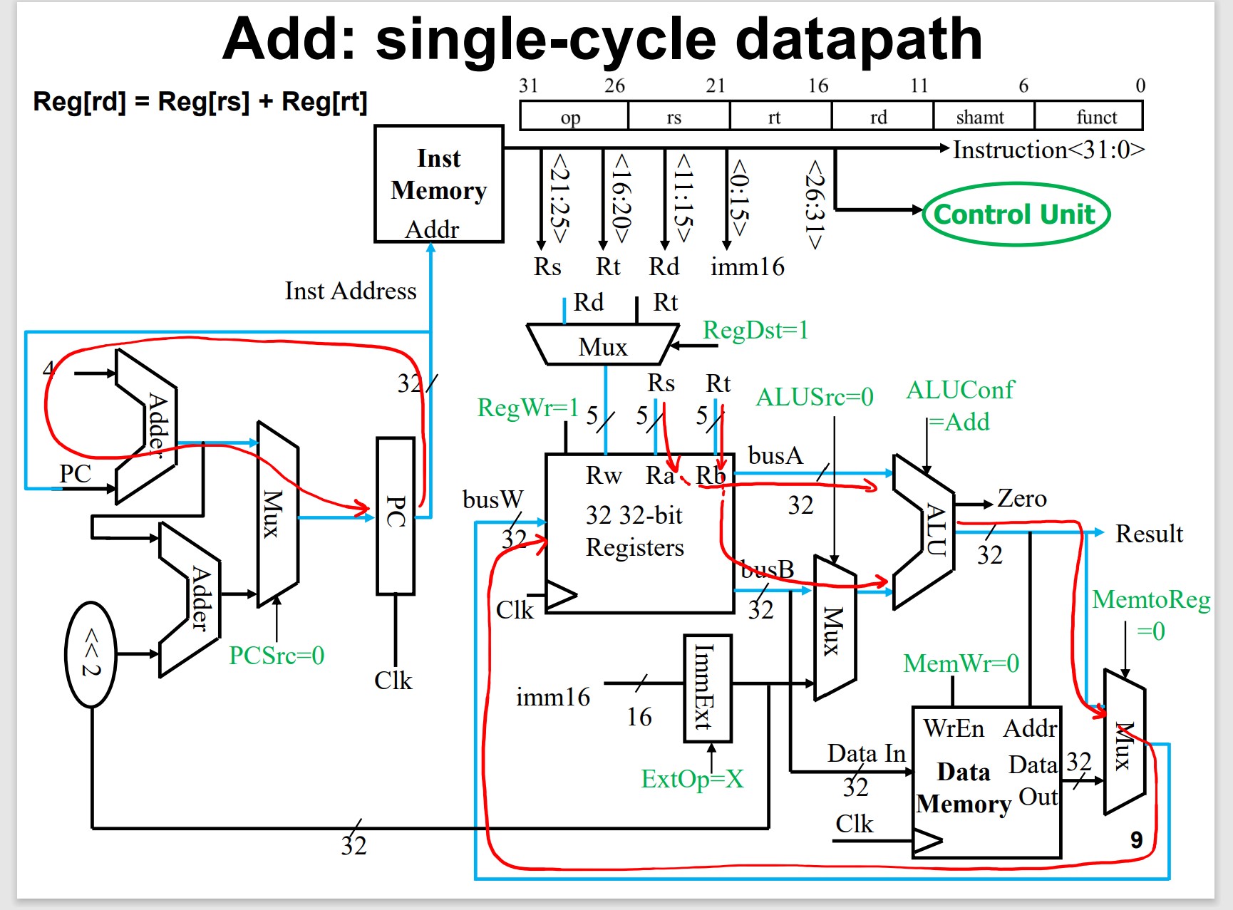
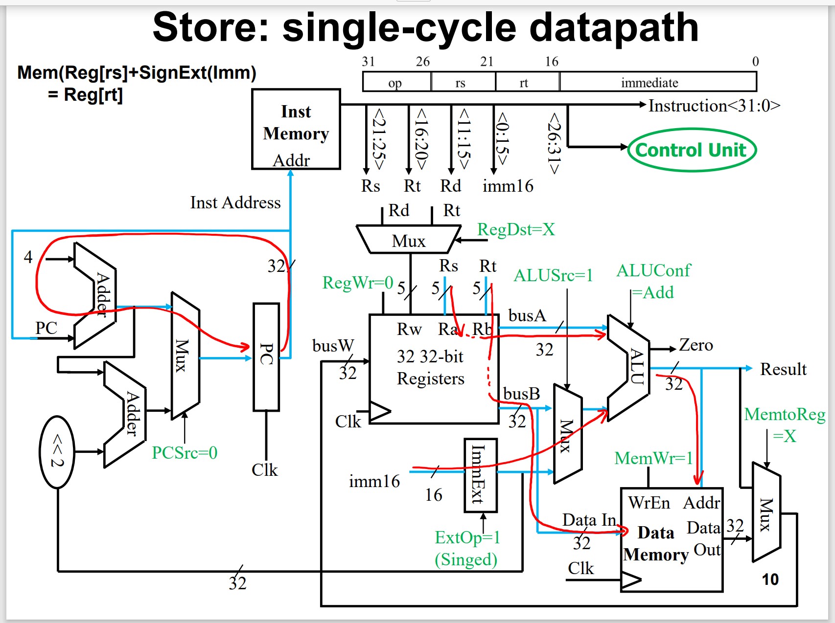
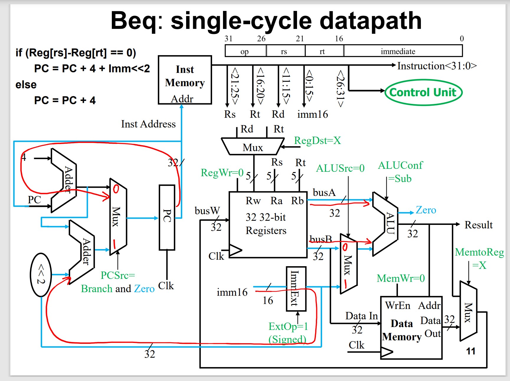
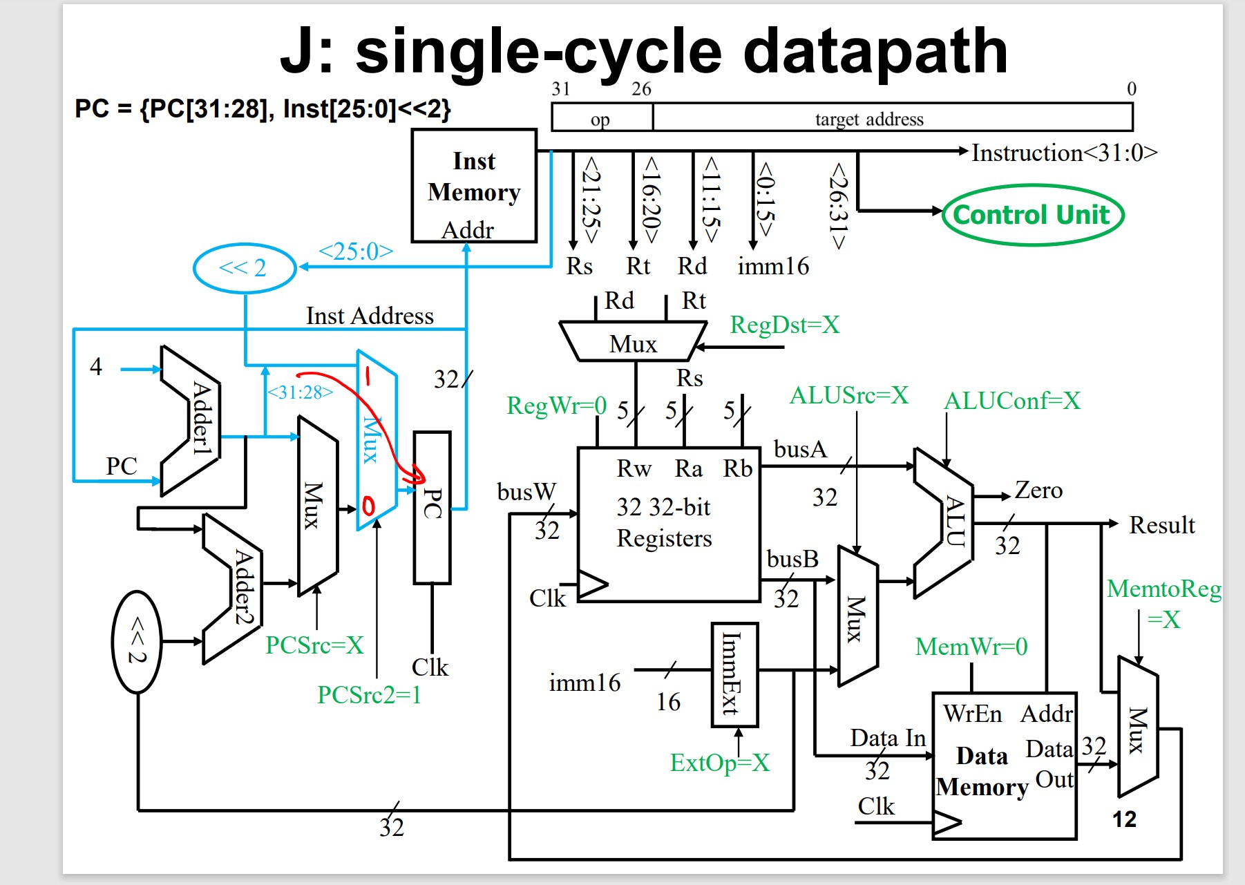
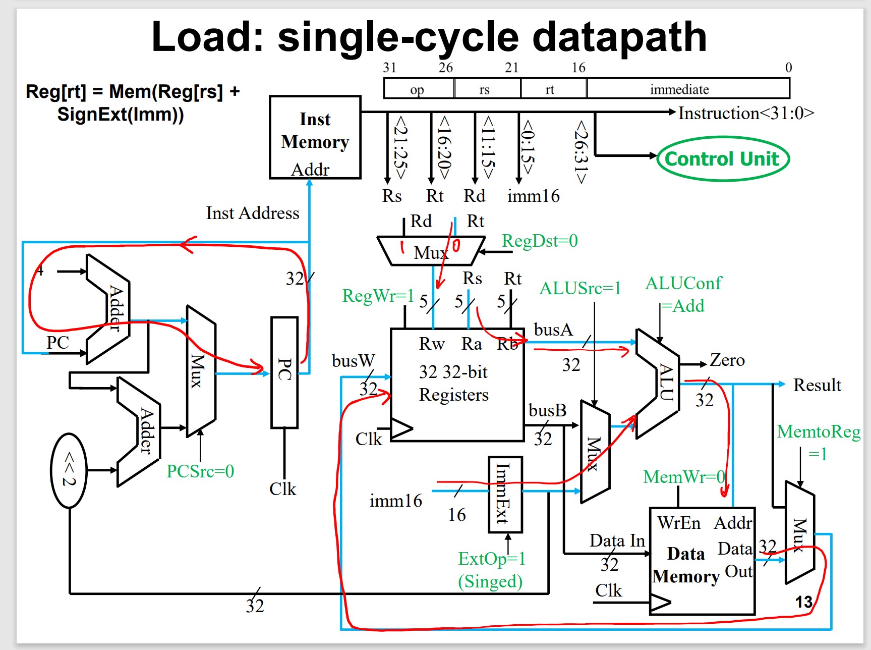
Load Operation Takes MUCH LONGER!!!
Multi-Cycle Processor
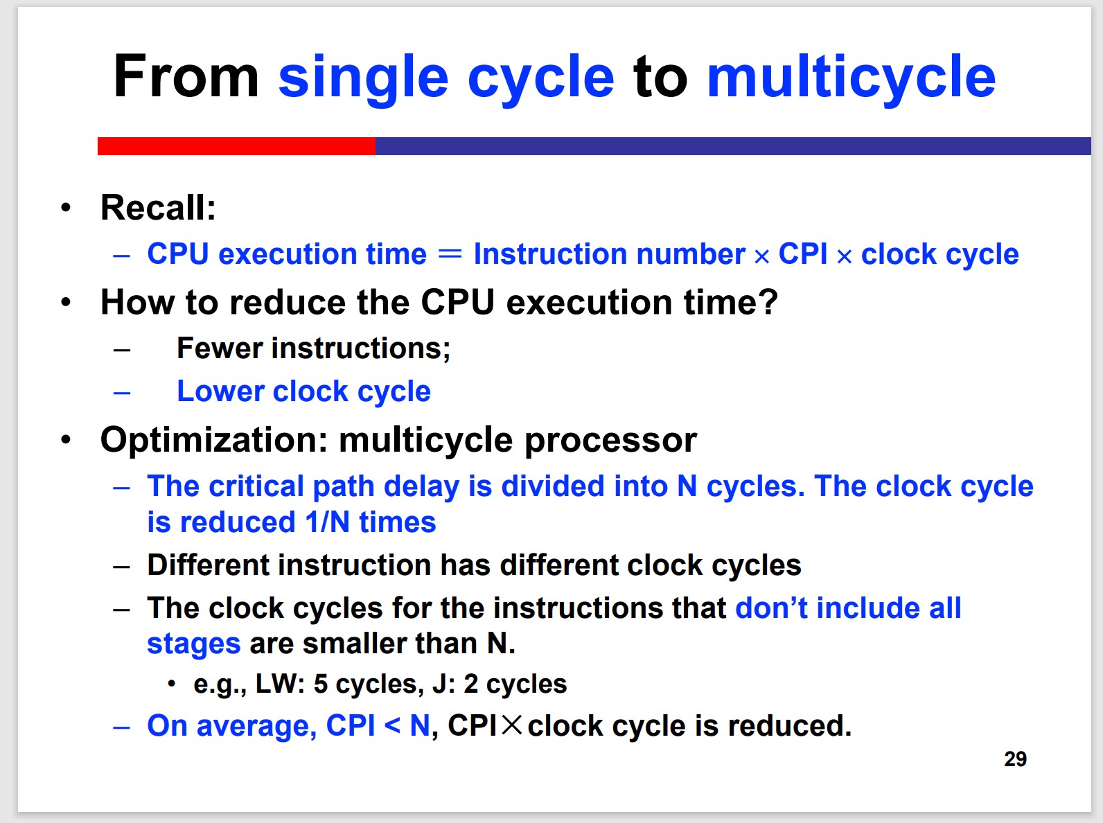
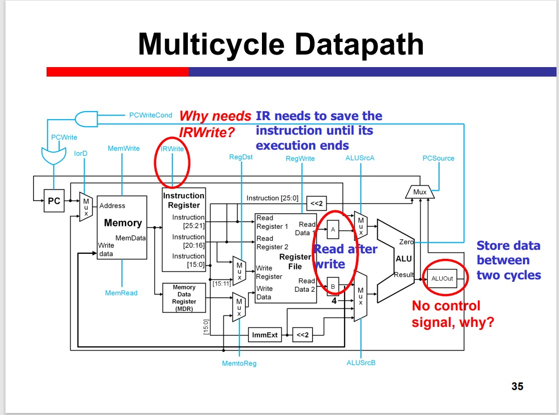
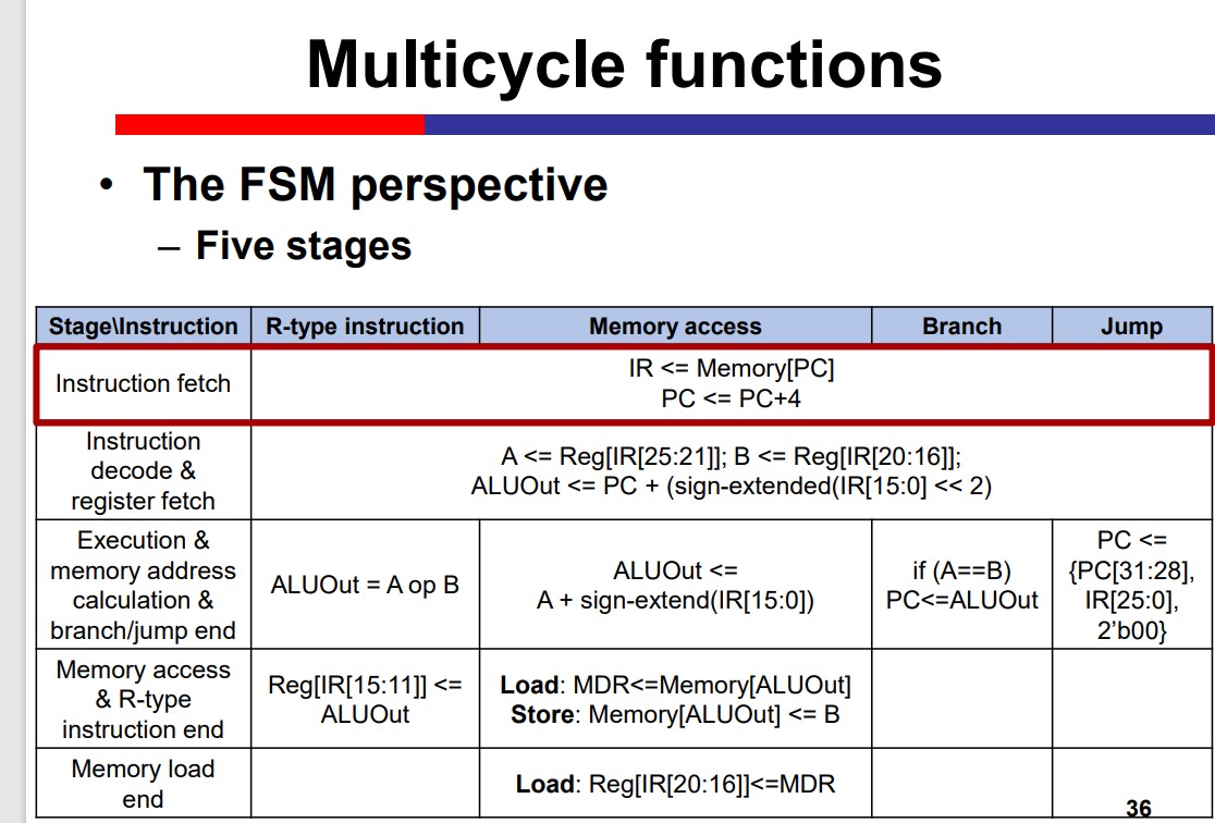
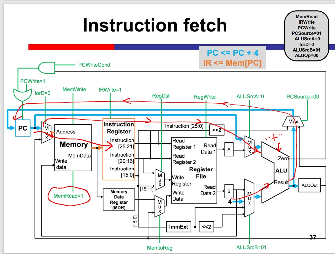
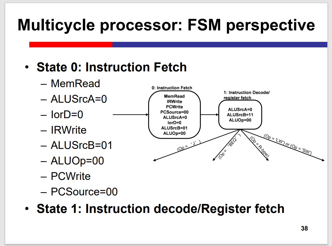
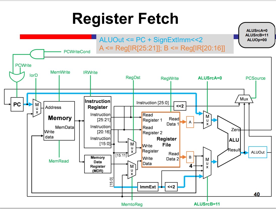
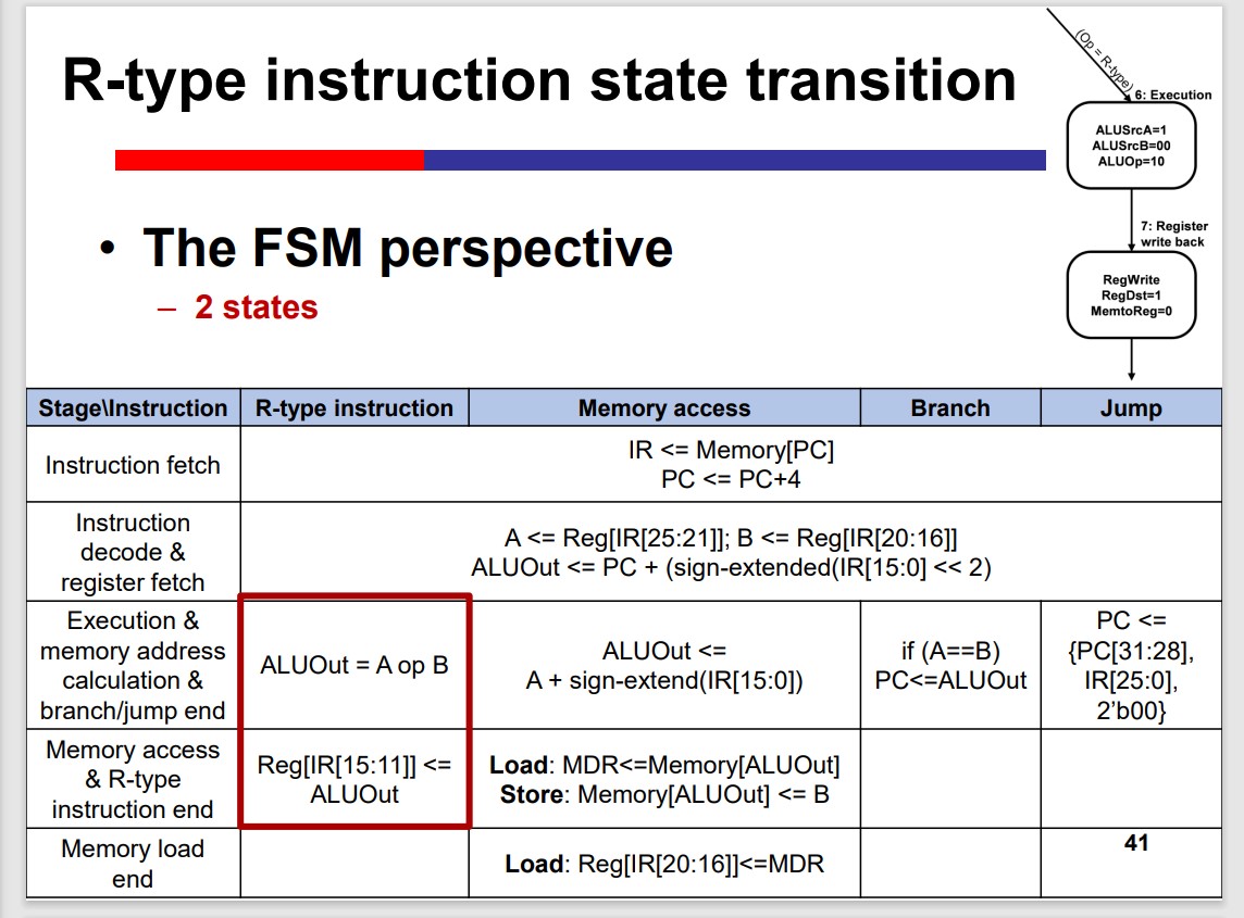
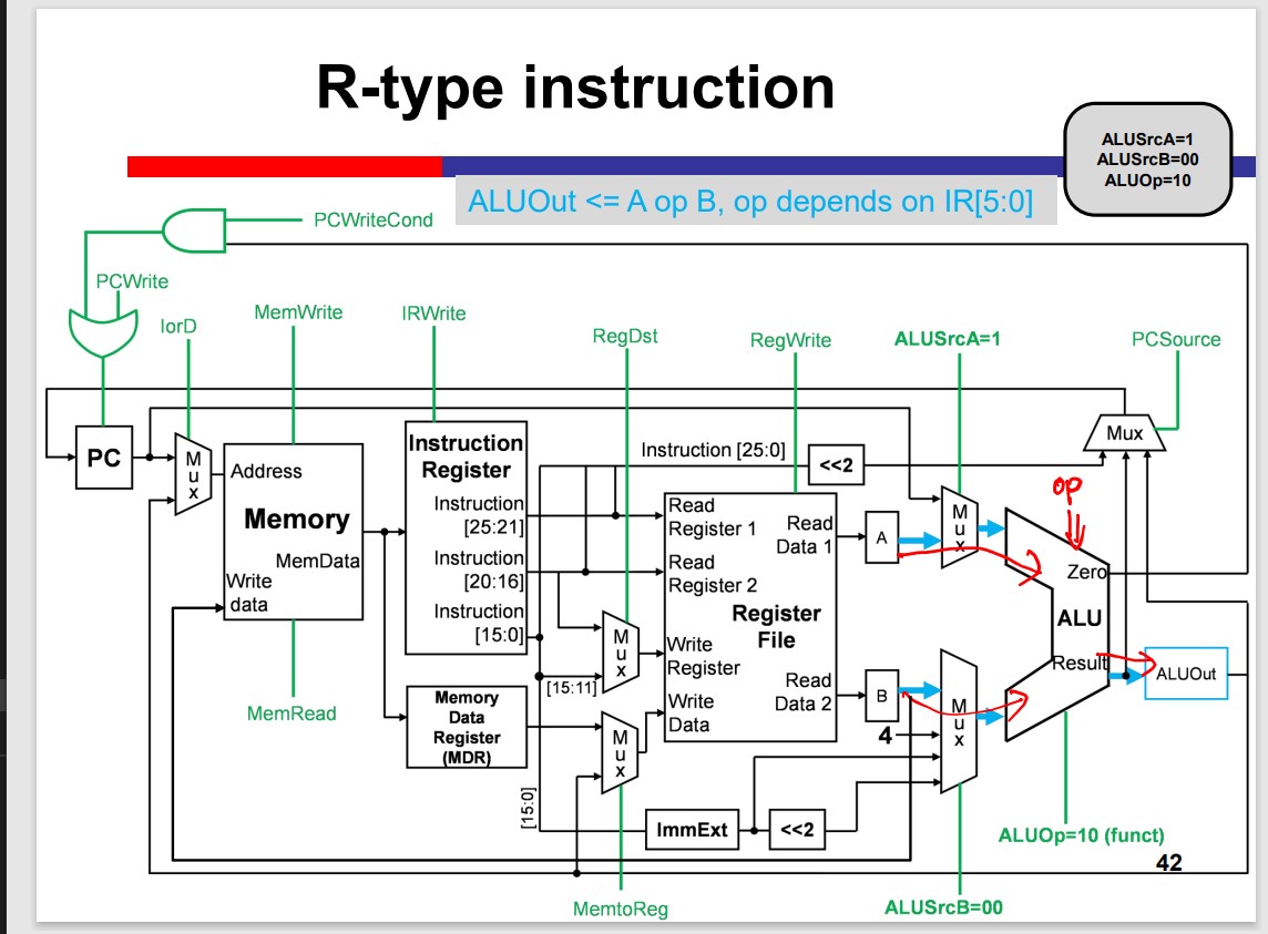
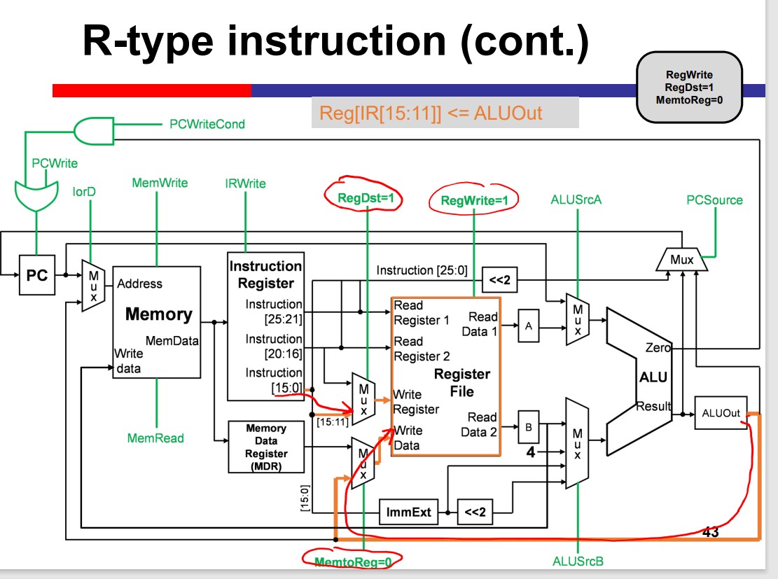
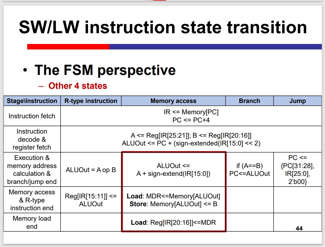
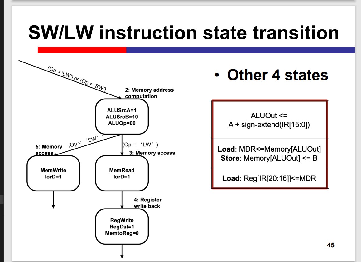
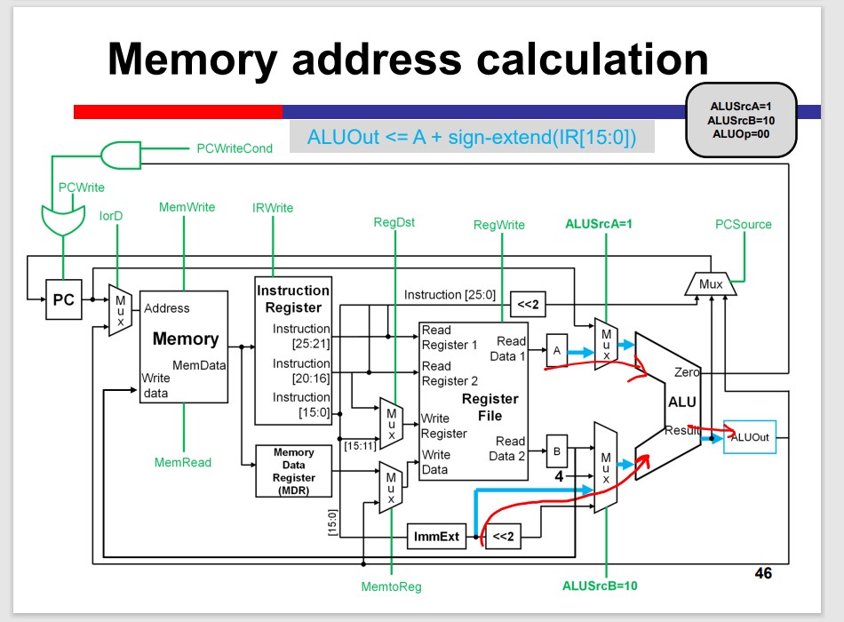
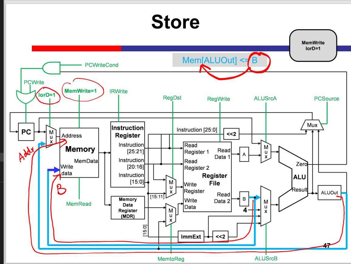
The Multicycle processor processes different inst. in different cycles. Thus, it can avoid the time limitation by the slow instruction.
Modules on th datapath can be used multiple times within an inst. That is Module reuse.
Performance improvement depends on the detailed delay. The multicycle is not necessarily faster than the single cycle.
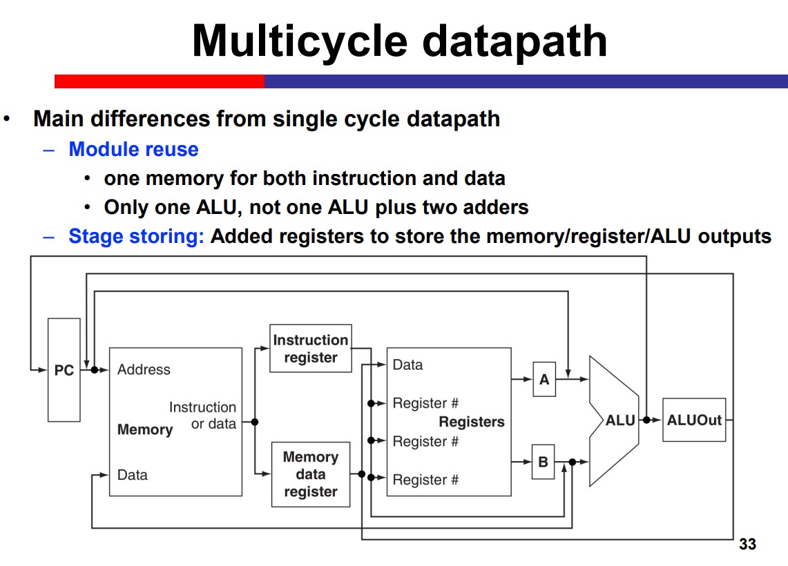
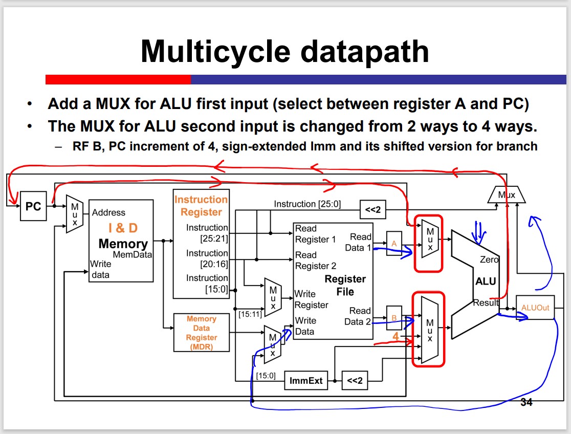
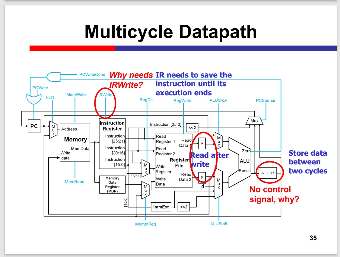
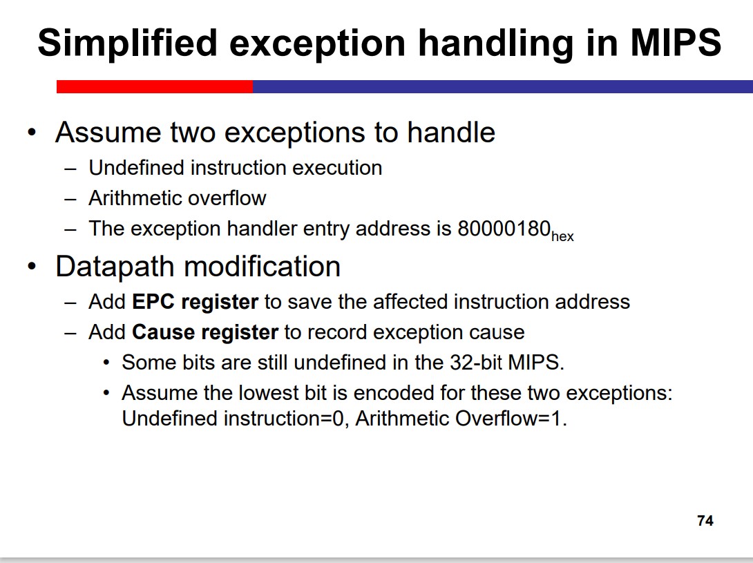
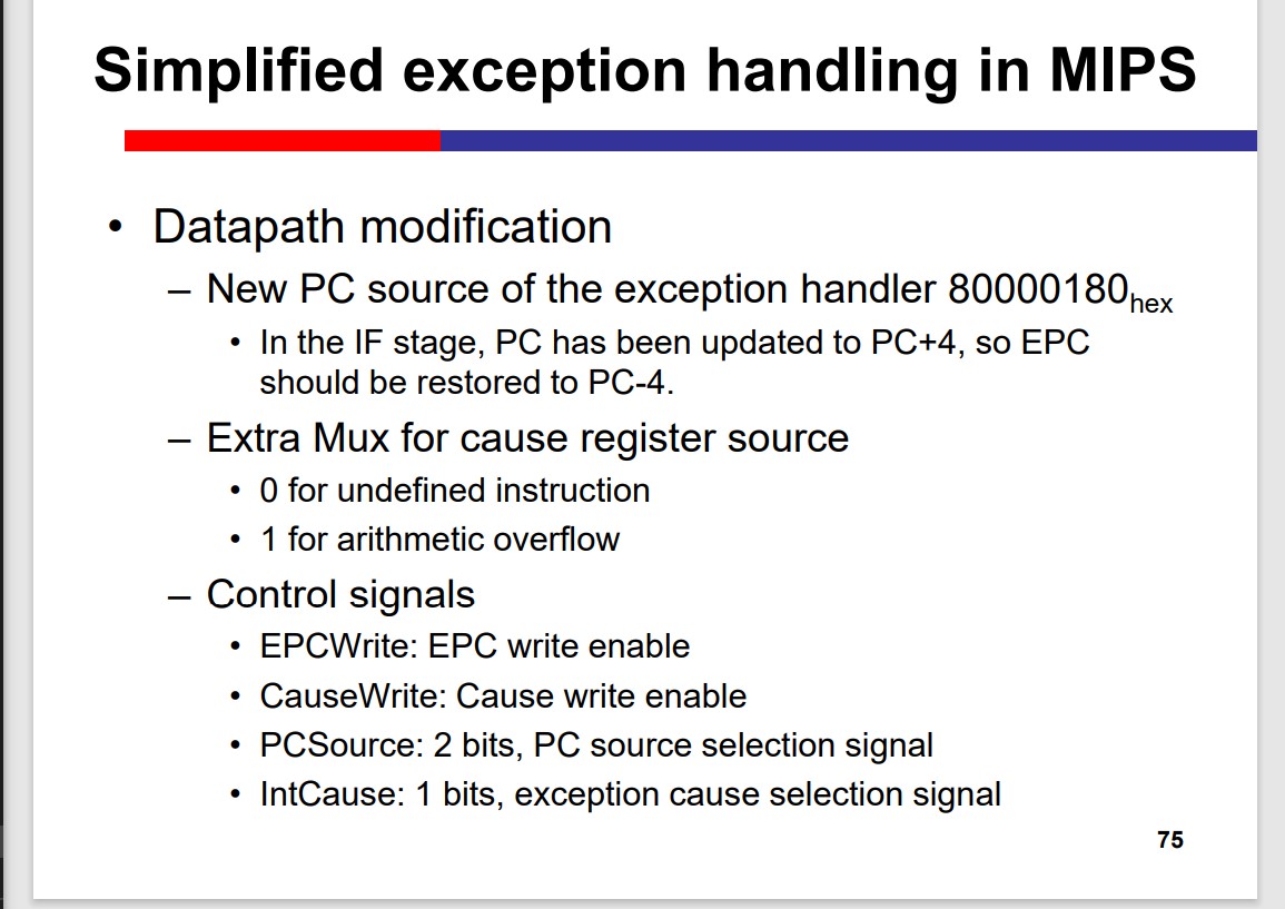
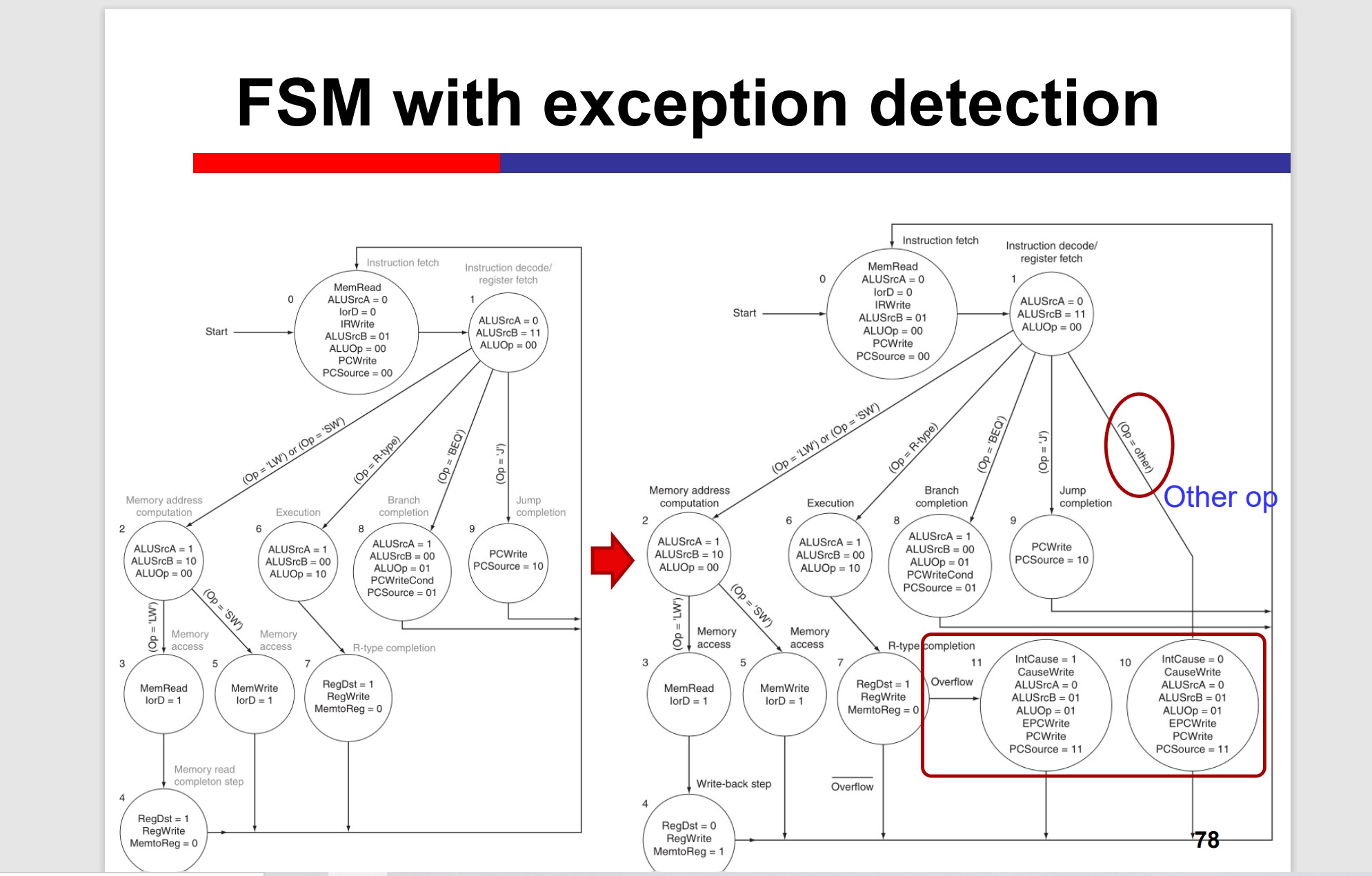
Exception and Interrupt
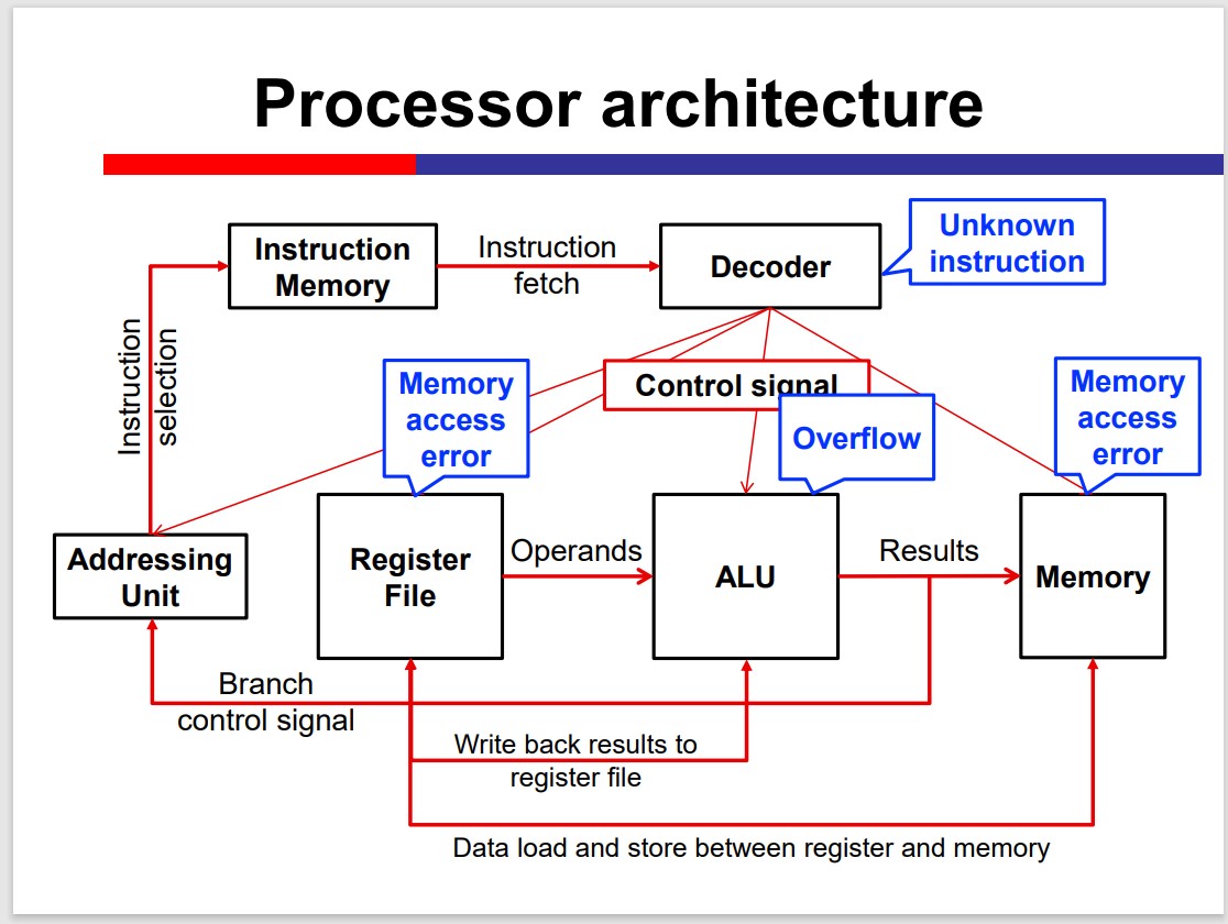
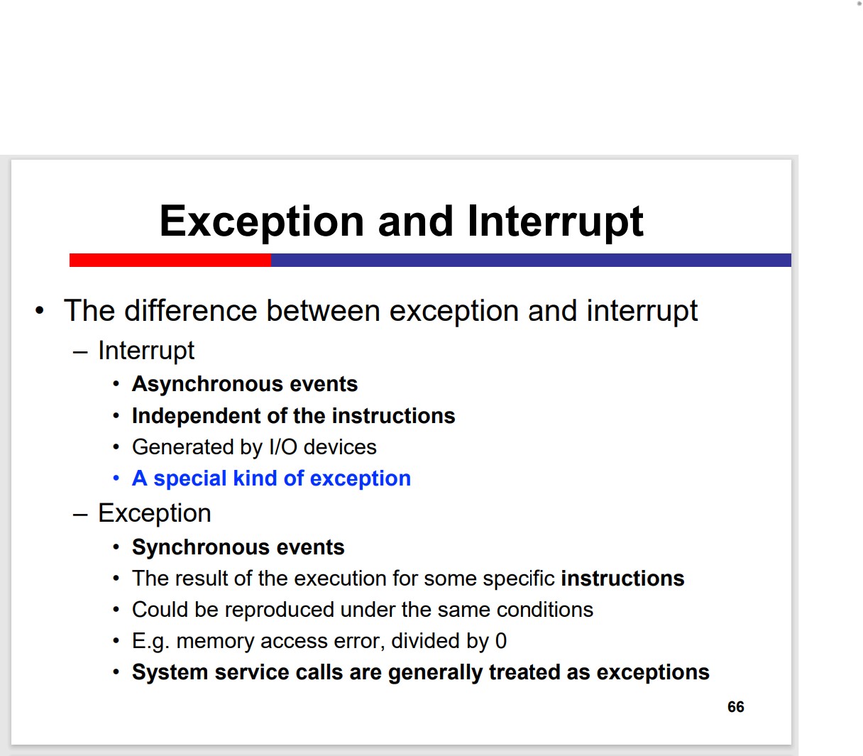
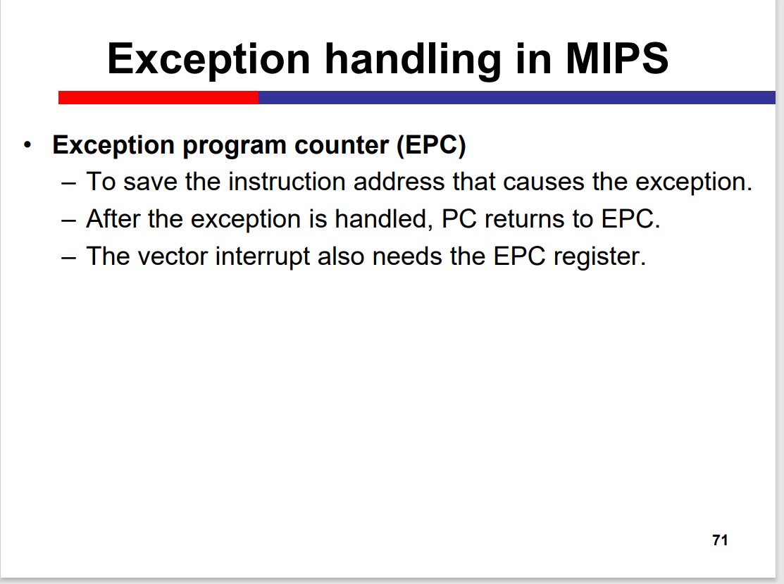
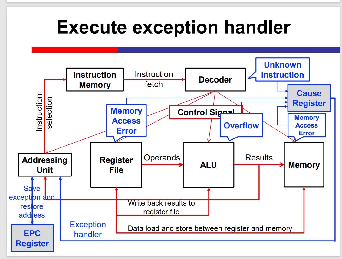
Generally, exceptions and interrupts are events that can change the normal instruction execution flow (other than branches and jumps).
Exception
– Internal unpredictable events such as overflow.
Interrupt
– External unpredictable events such as I/O.

Pipelined processor
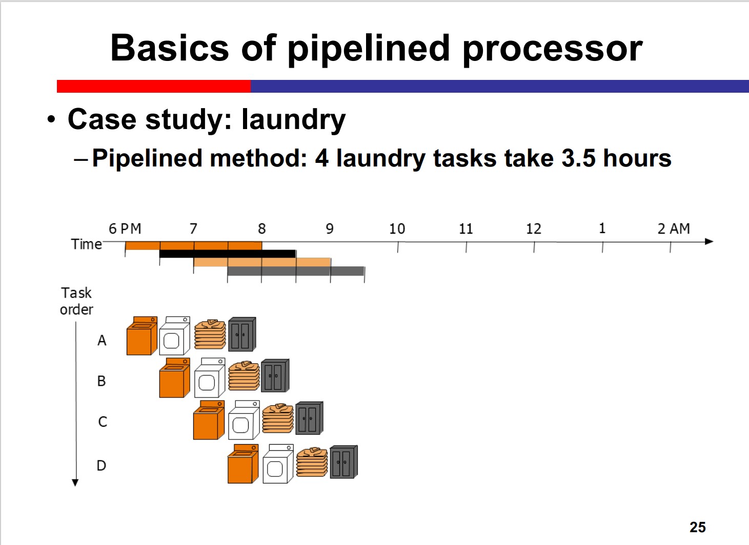
Pipeline means spatial and temporal reuse.
Divide a complex task into several sub-tasks to
execute sequentially, and assign each sub-task to
dedicated hardware
Different sub-tasks of multiple tasks can be
processed simultaneously to improve the
performance
• Time-division multiplexing: the same resource is reused through
different cycles
• Space-division multiplexing: multiple resources are reused
within one cycle
Pros: improved efficiency
Cons: Some inst. depends on the former inst.. However, the former inst. has not finished yet, if the prediction of branch is wrong, time is wasted.
Instruction-Level Parallelism (ILP)
– Execute multiple instructions in parallel
– One mainstream approach to CPU performance improvement
Basic Techniques
– Pipelining: instruction execution is divided into several stages, and
each stage can be processed with the other stages (of other
instructions) simultaneously
– Superscalar: multiple dedicated functional units are equipped so
that CPU can receive & execute more instructions within one cycle.
– Very Long Instruction Word (VLIW): each instruction consists of
multiple segments to utilize the processor resources independently.
5 stages in MIPS:
- Instruction Fetch (IF)
- Instruction Decode / Register File
- ALU Execution(EX)
- Memory Data Access(MEM)
- Reg Write-Back(WB)
Latency of the stages in the pipeline should
be as equivalent as possible, why?
–The pipeline performance is bottlenecked by the stage
of the longest latency
Metrics of pipelined processors
- Throughput(TP): Executed instruction # per unit time
- Max throughput: The throughput of a steady-state pipeline with a continuous instruction input stream
- Real throughput: The throughput of the pipeline executing task with finite instructions
Real TP:
$$ TP = \frac n {T_k} = \frac{n}{(n+k-1)\Delta t} $$Max TP:
$$ TP_{max} = \lim_{n\rightarrow\infty}\frac{n}{(n+k-1)\Delta t} = \frac{1}{\Delta t} $$Speed up Execution time ratio between w/o or w/ pipelining.
$T_0$ : execution time without pipelining $T_k$ : execution time with k-stage pipelining(assume each stage has the same latency) $$ \frac{T_0}{T_k} $$Real speedup:
$$ S = \frac{nk\Delta t}{(n + k - 1)\Delta t} = \frac{kn}{n + k - 1} $$Max speedup:
$$ S_{max} = \lim_{n\rightarrow \infty}\frac{kn}{k + n - 1} = k $$Pipelined datapath
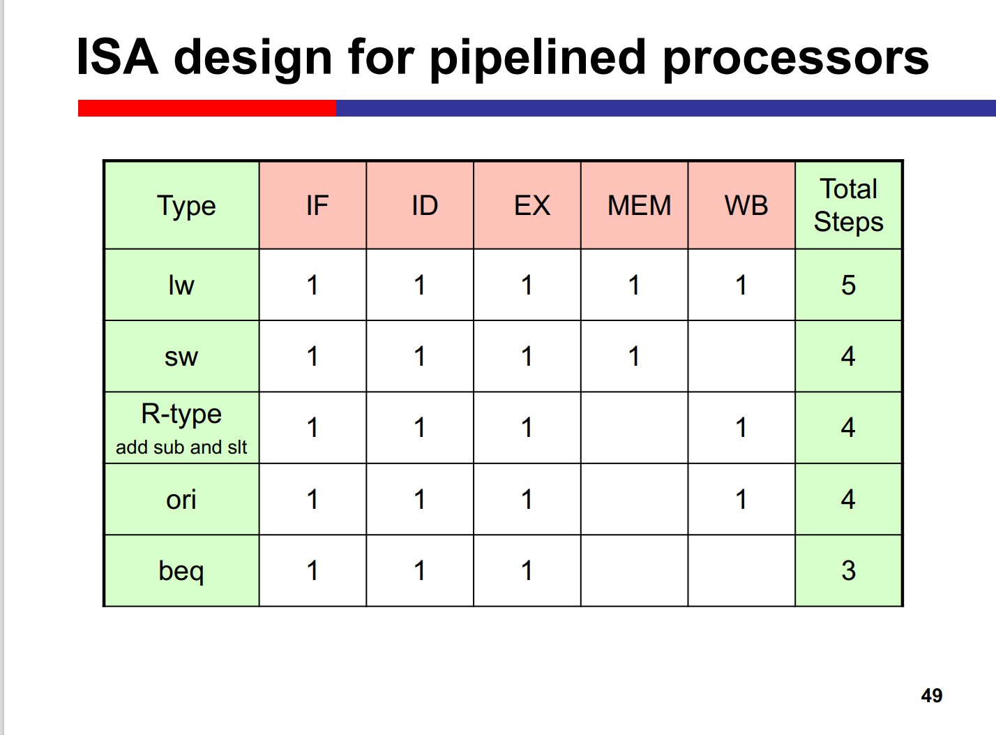
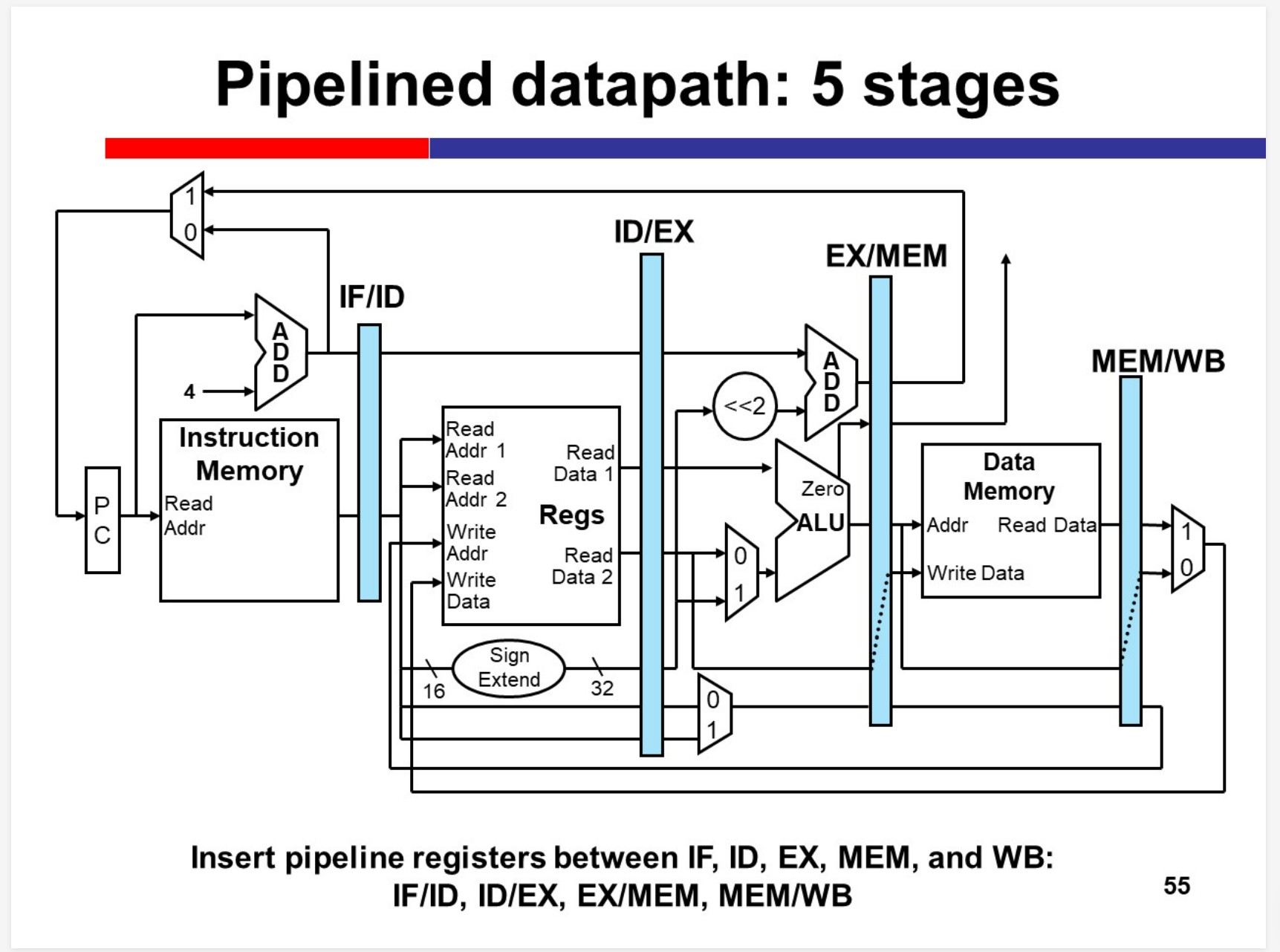
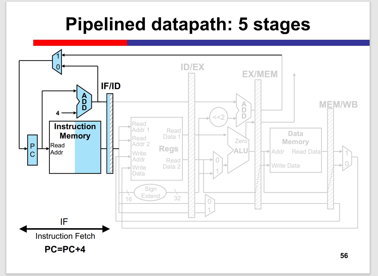
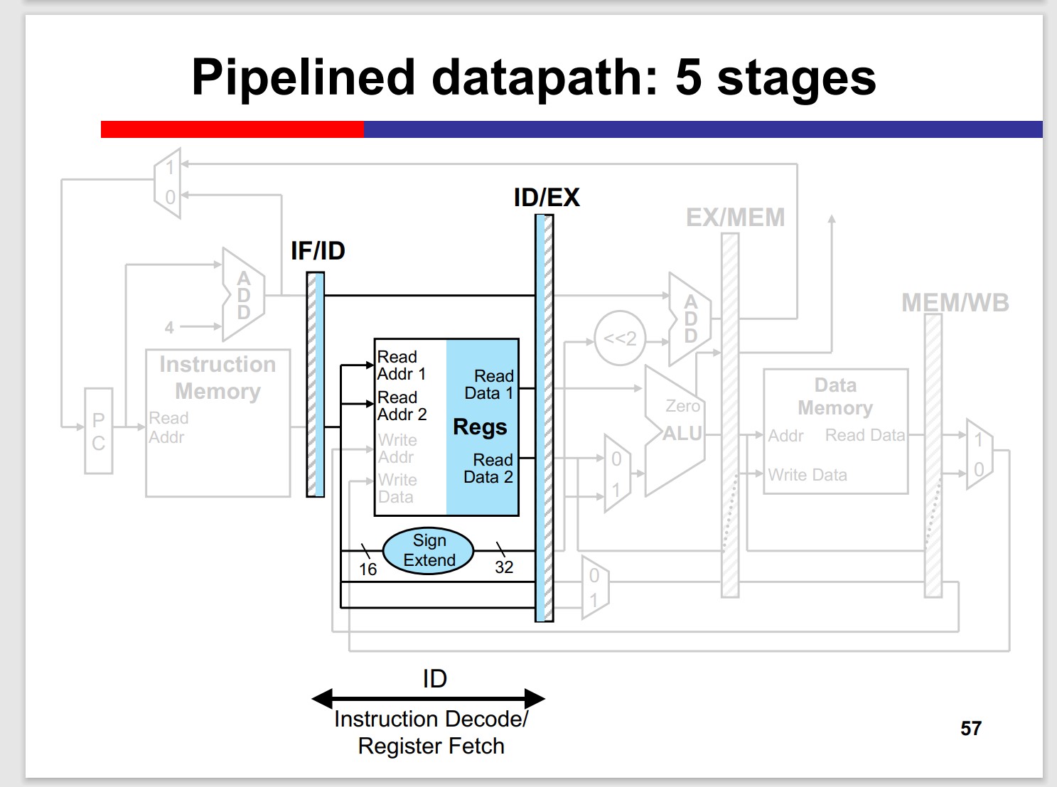
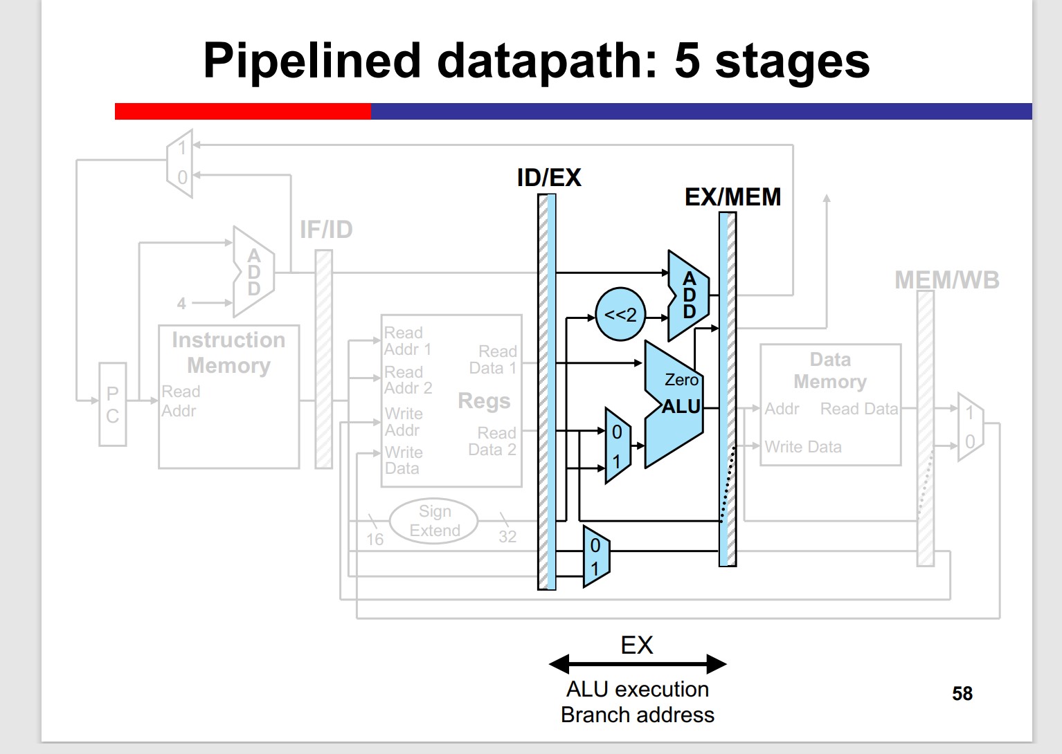
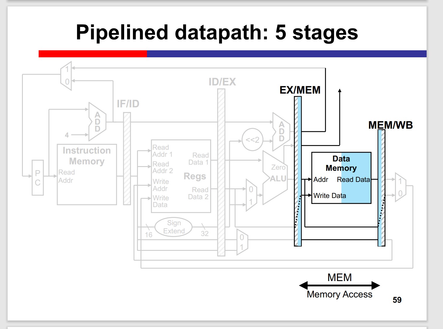
Many inst. doesnt need MEM stage, but the stage can’t be skipped, since it may “collide” with the previous inst.
Q: How to get the control signals in each stage?
Control signals are generated at ID/RF stage.
Control signals flow in the pipeline: use when needed; reserve when subsequent stages needed; discard when not needed any more.
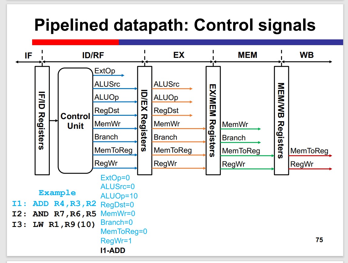
Why RegDst Doesnt needed in the stages after EX?
The RegDst is used to select the destination register. However, the destination register is determined in the EX stage. Thus, RegDst is not needed in the stages after EX.
Sometimes this can cause trouble:
1 | LW R2, R9(10) |
The R4 is accessed before it updates.
Hazard in the pipeline
Structural Hazards
Two instructions acquire the same hardware resource simultaneously.
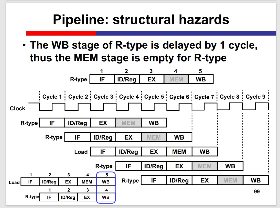
Solution:
- Add resources: separating PC+4 from ALU; Harvard architecture
- Adjust stages: add MEM
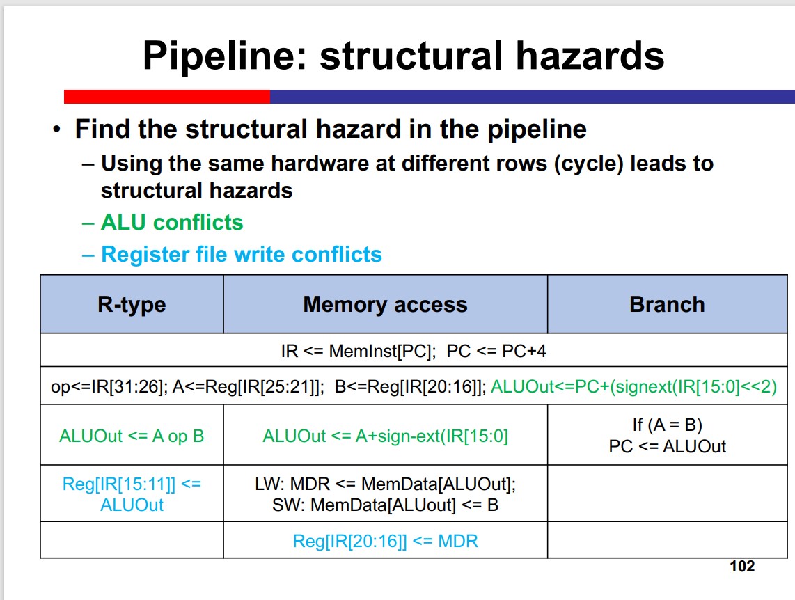
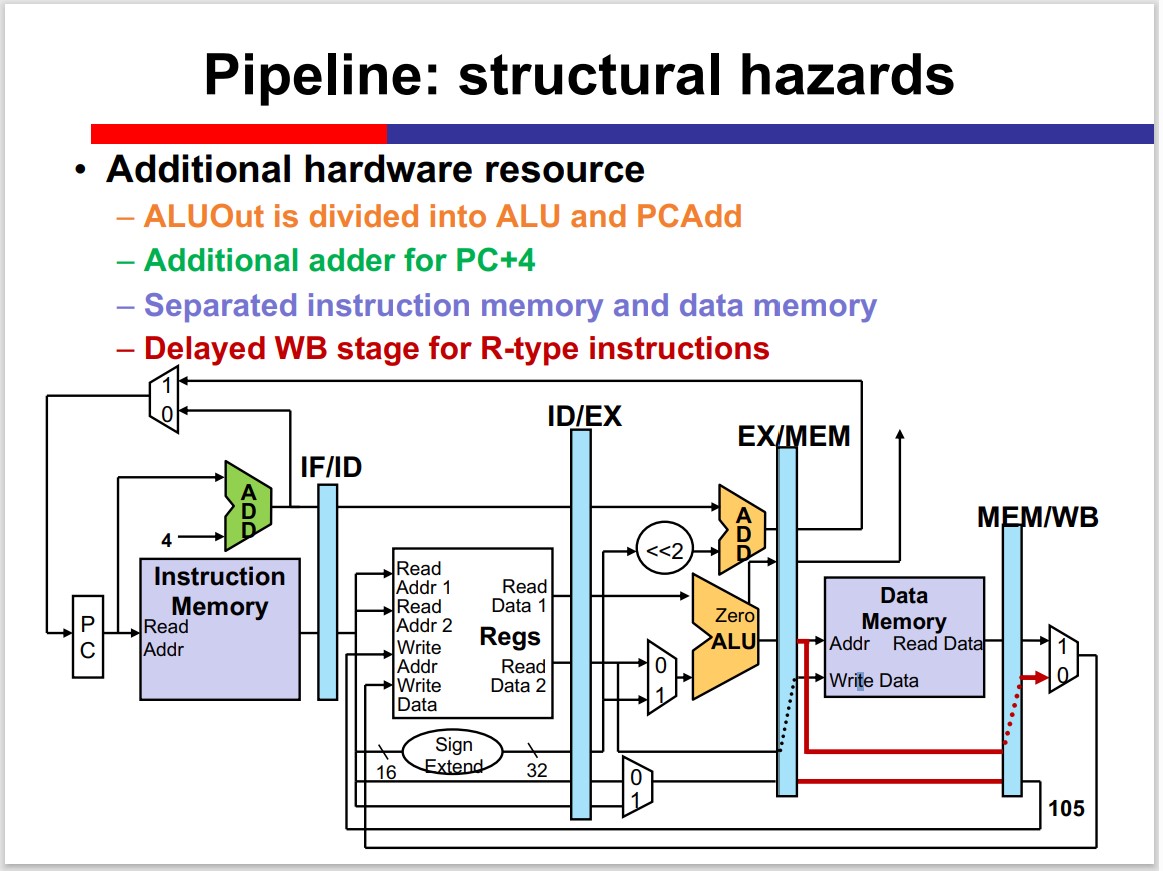
MIPS is born to be pipelined: the problem of structural hazard is solved by the structure of MIPS.
Data Hazards
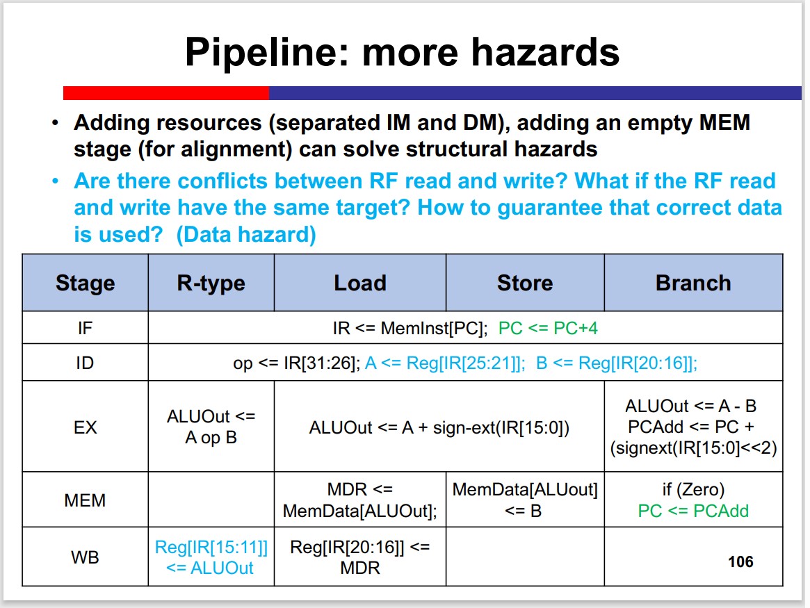
2 solutions:
Stalling
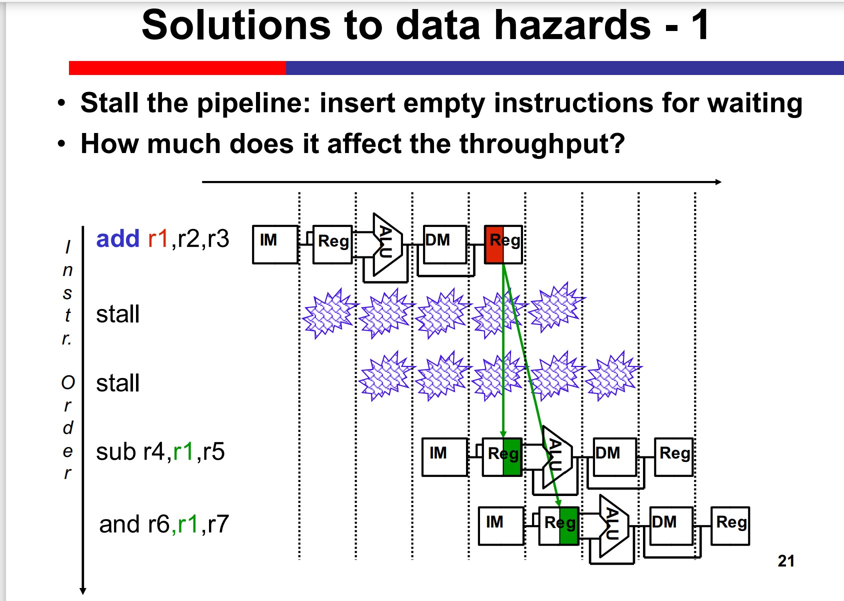
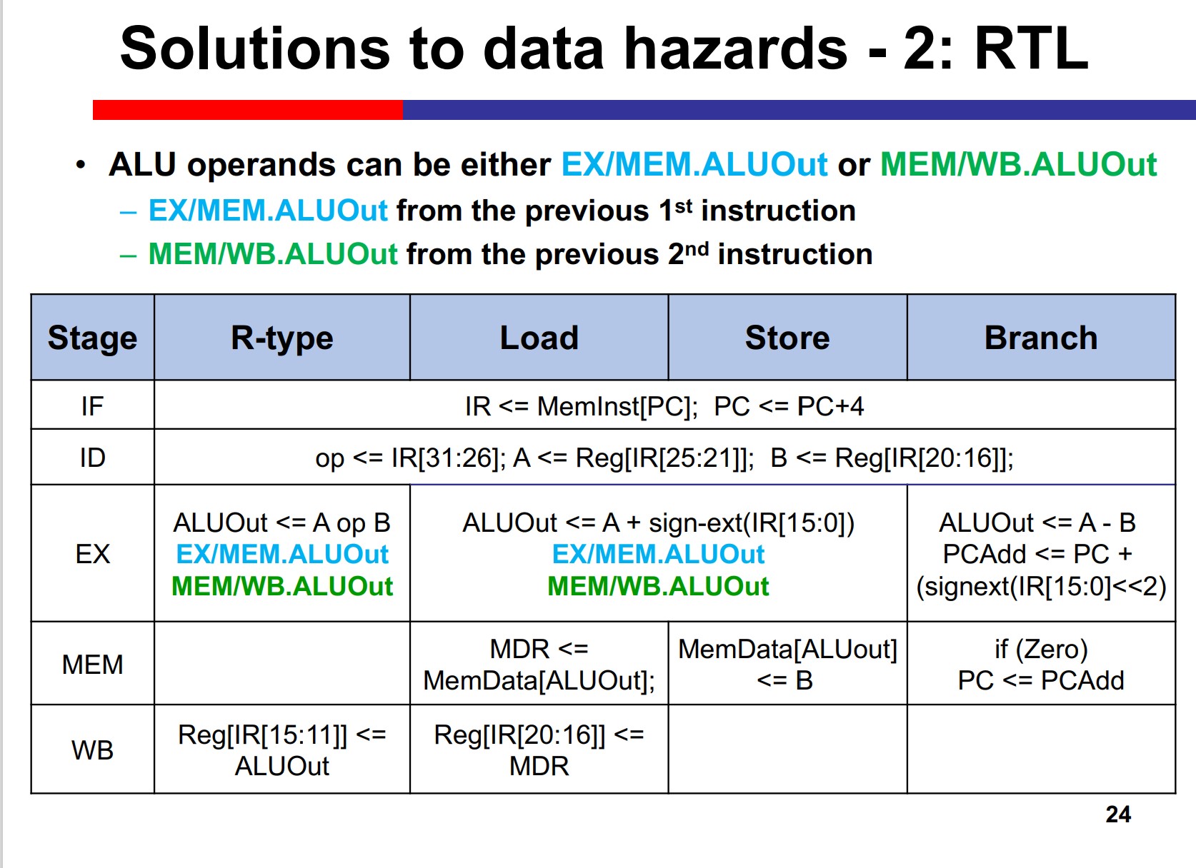
Forwarding(Bypassing)
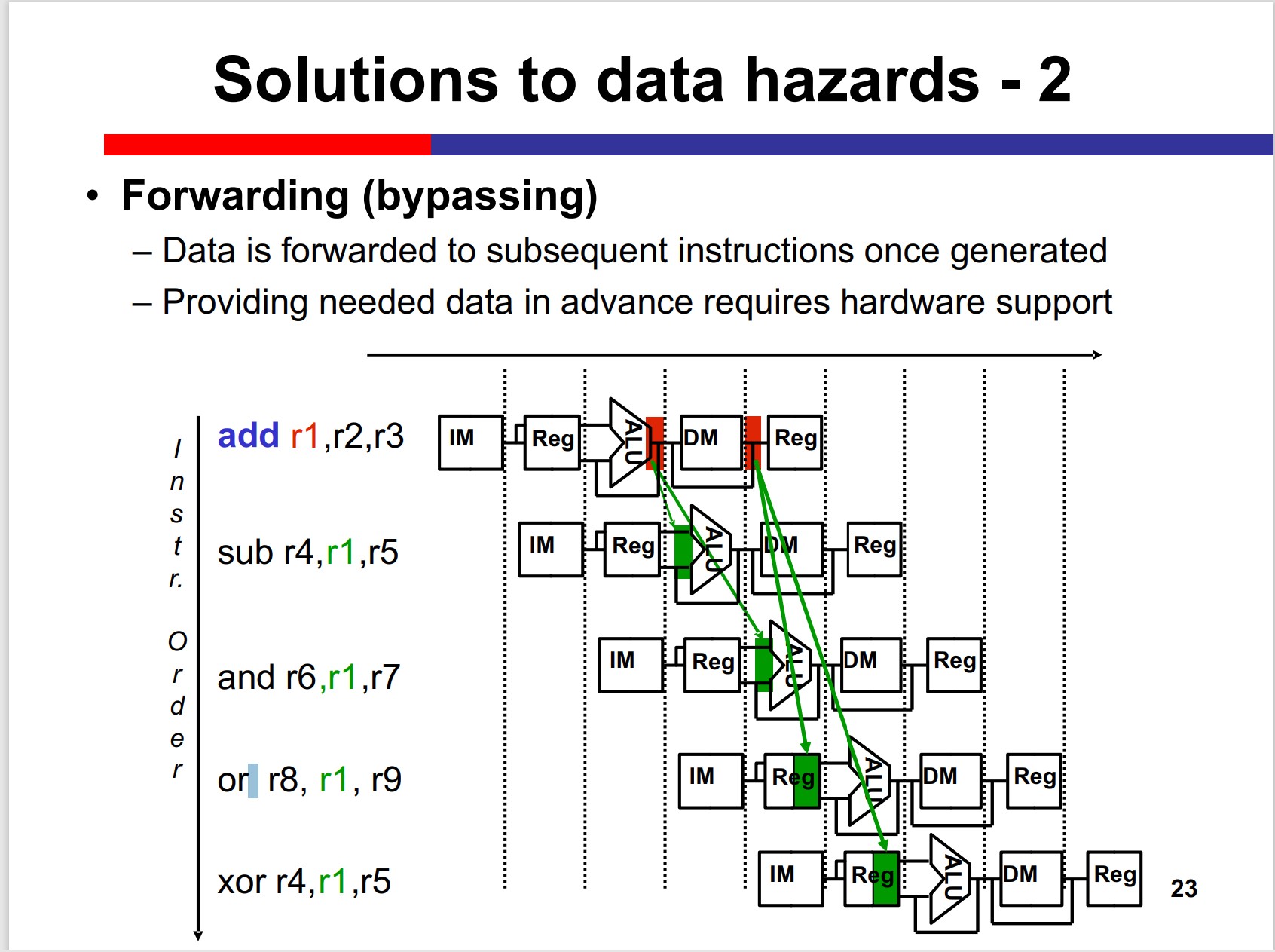
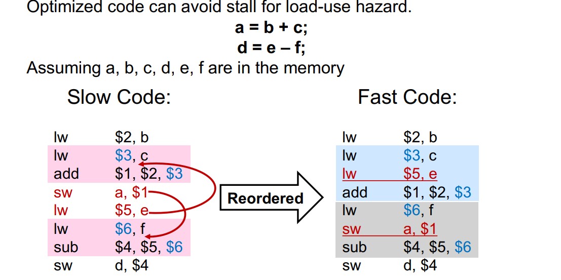
But, load uses hazard emerges:

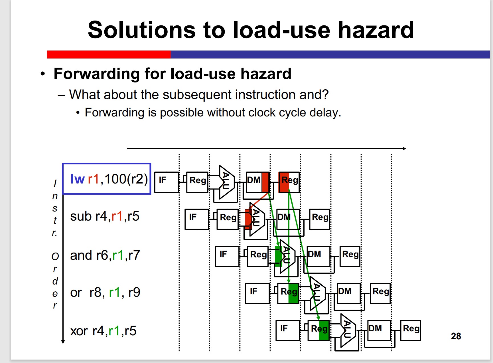
Still, a nop needed to stall the pipeline.
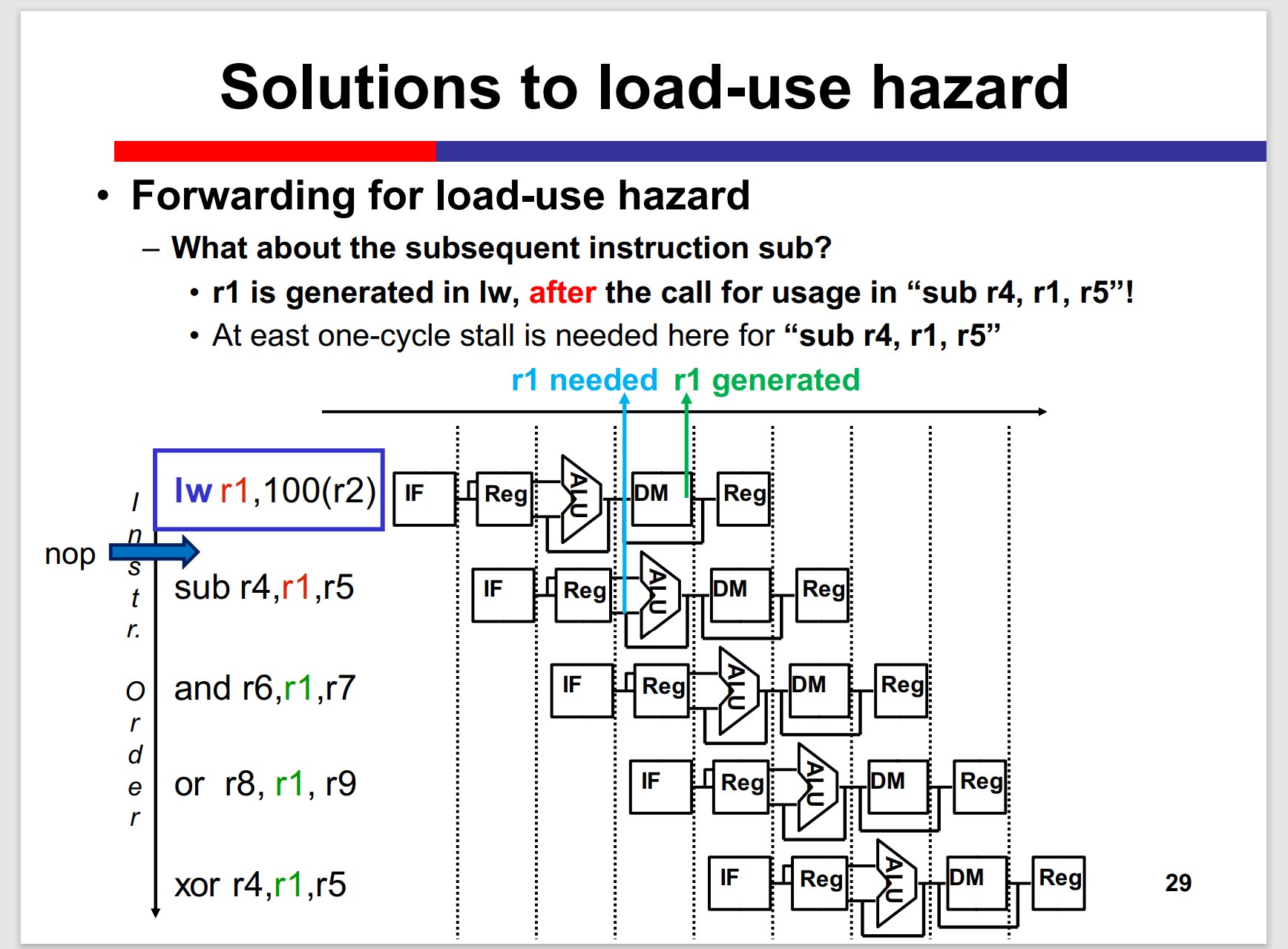
Is there any possibility to eliminate the stall?
Yes, if the MIPS code can be optimized.
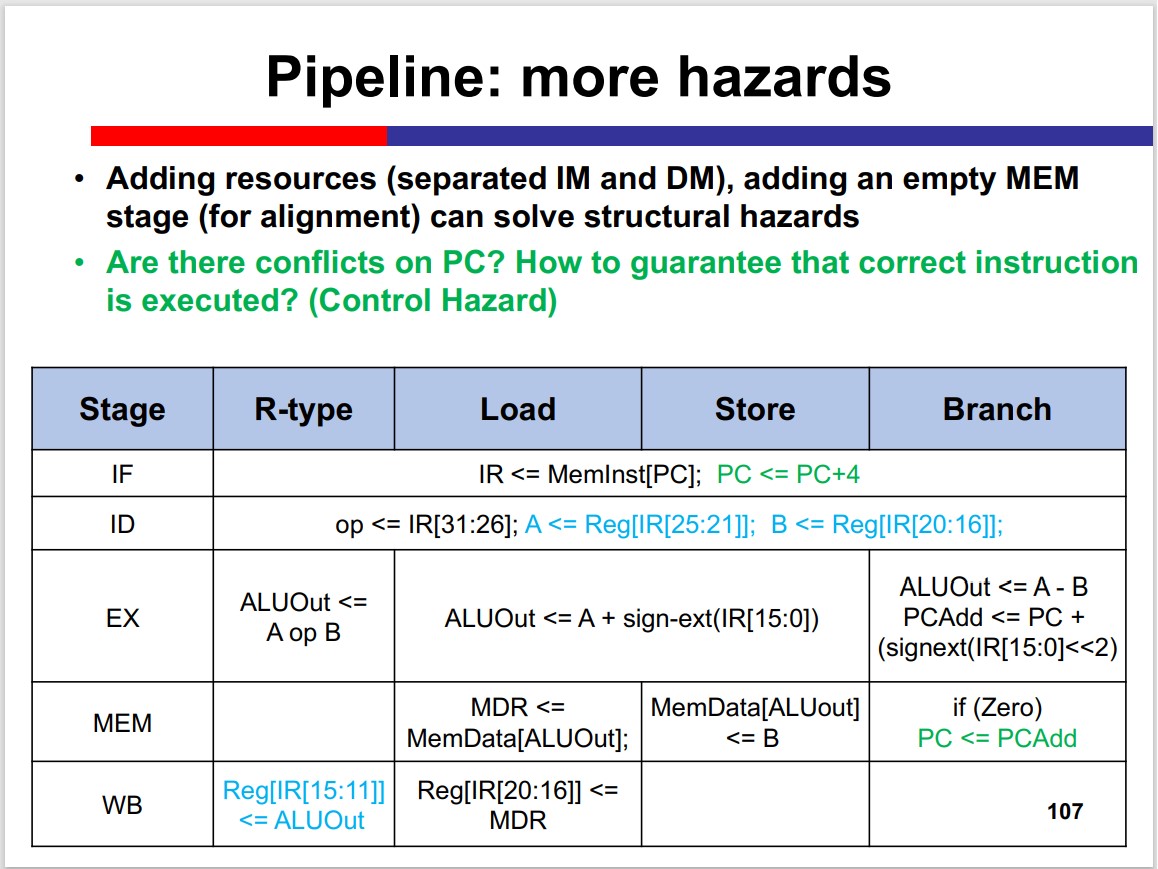
Control Hazards
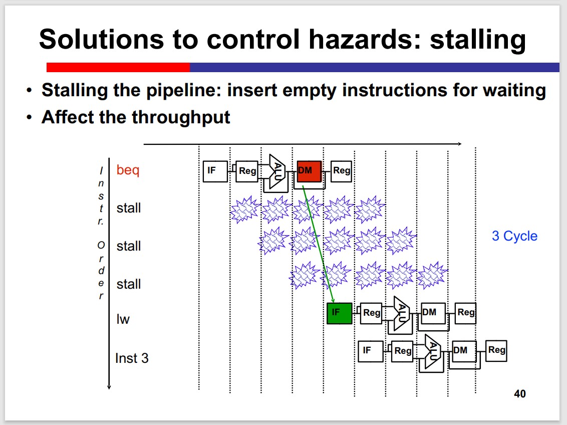
Stalling
Forwarding
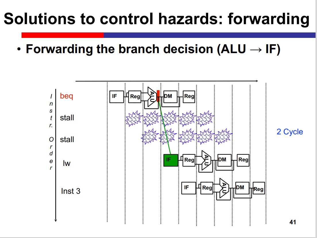
If Move the branch decision to ID stage:
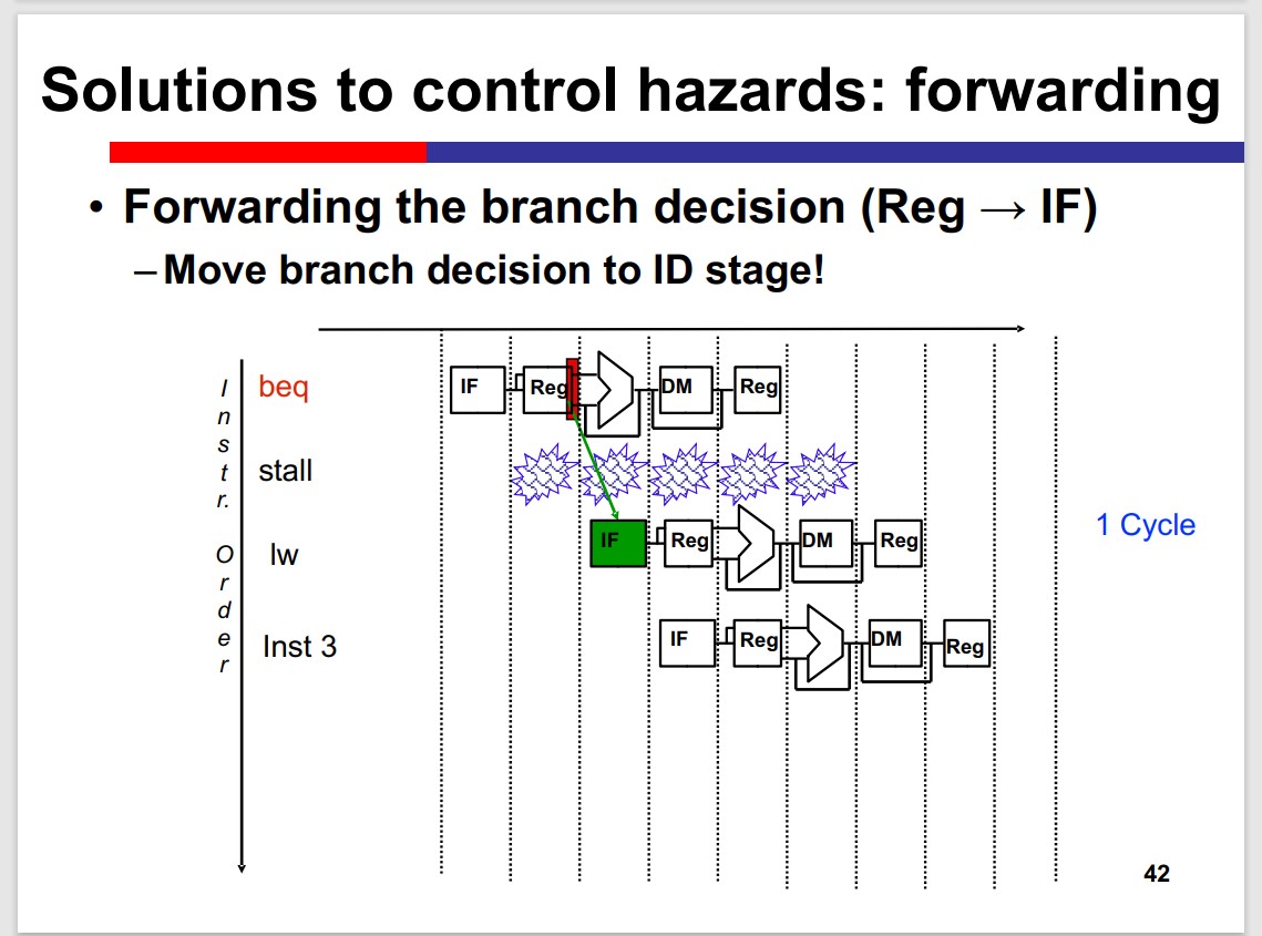
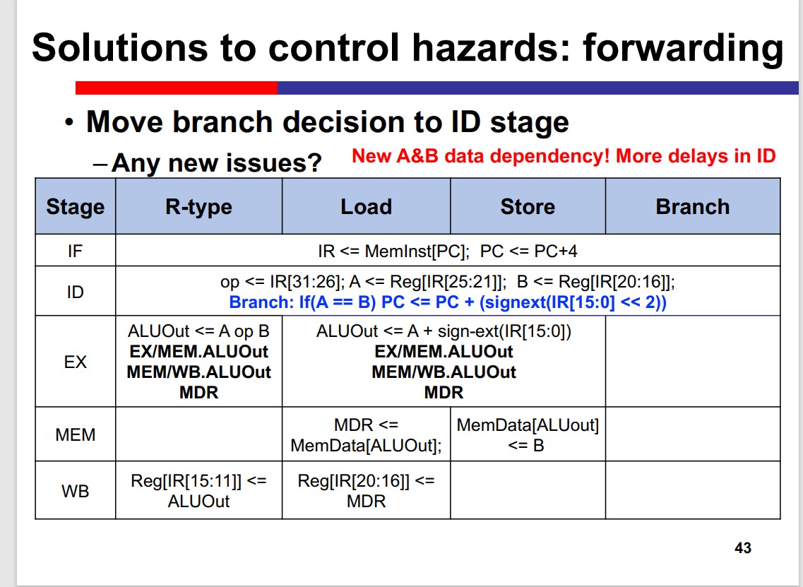
Delay slot
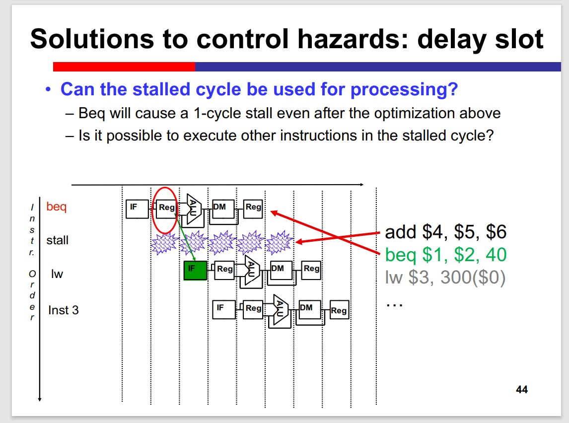
Prediction
Static Branch Prediction
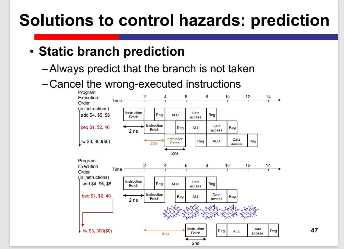
Cancel the effect caused by false prediction.
Dynamic Branch Prediction
- History-based dynamic prediction
- Using runtime behaviour to predict future branches
At IF stage, there are Branch History Table(BHT) and Branch Target Buffer(BTB).
beq at IF stage
• Look up if the instruction address is in BHT and BTB.
• If not in, create a new entry. If in, check whether the
branch is taken at the last time. If taken, send the target
address to PC as the next address for IF.
–beq at ID stage
• IF stage will fetch instruction based on the predicted
target address
Implementation of the Pipiline
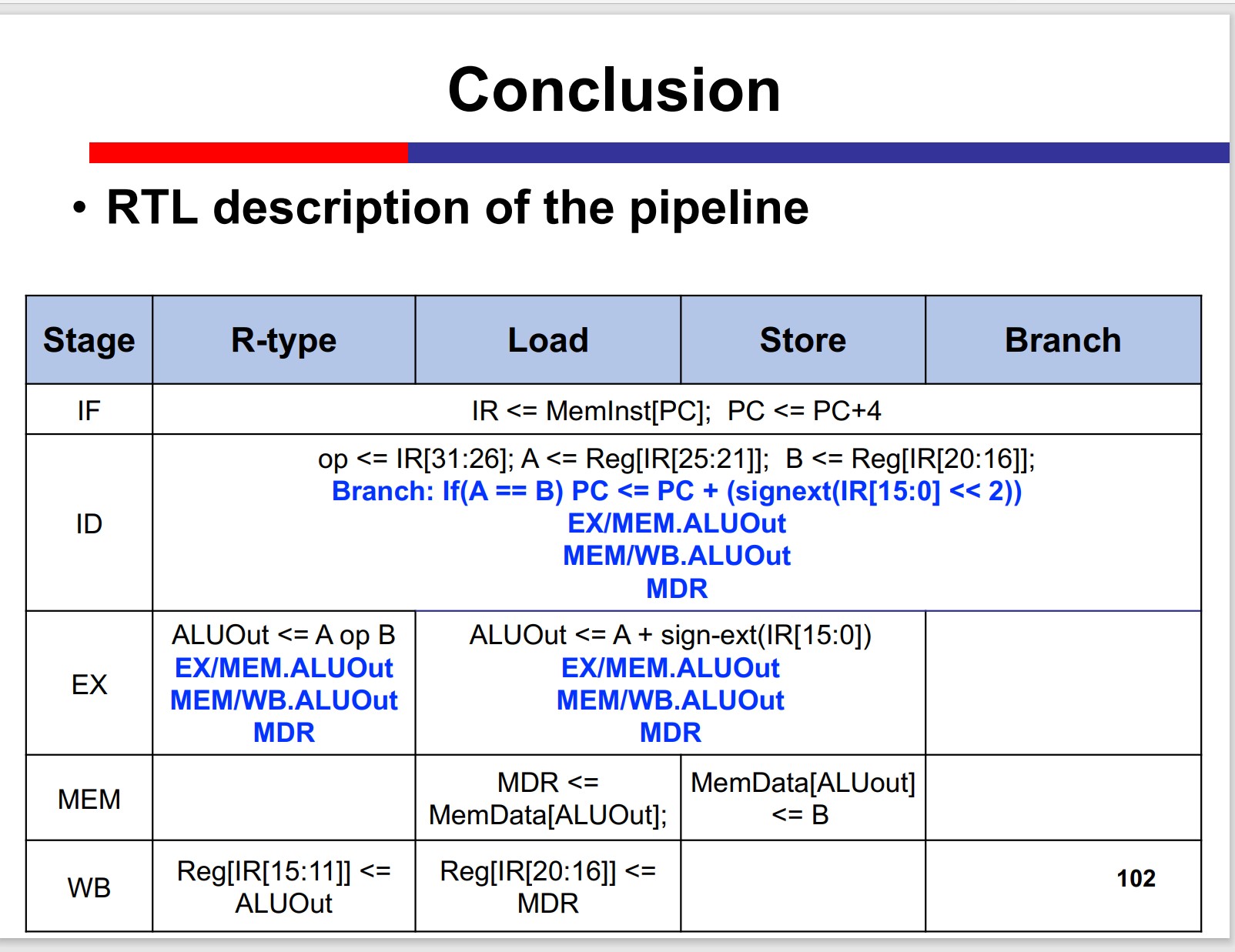
Data hazard
Forwarding
EX/MEM hazard
1 | if (EX/MEM.RegWrite |
MEM/WB hazard
1 | if (MEM/WB.RegWrite |
load-use hazard
We have to stall the pipeline for one cycle.
Condition: if (ID/EX.MemRead and ((ID/EX.RegisterRt == IF/ID.RegisterRs) or (ID/EX.RegisterRt == IF/ID.RegisterRt)))
How to stall?
Stall & flush
PC & ID/IF: stall(Keep the control signals)
EX & MEM & WB: flush(Set the control signals to 0)
Control signals:
EX: RegDst, ALUOp1, ALUOp0, ALUSrc
MEM: Branch, MemRead, MemWrite
WB: MemToReg, RegWrite
1 | if {ID/EX.MemRead |
Special Case:
Memory-to-memory copy
1 | lw {% raw %} $1, 10($ {% endraw %}2) |
The stall is unnecessary. We can use forwarding to solve the problem.
Control Hazard
BEQ & J need 1 stall cycle.
Control hazards are not as frequent as data
hazards, but they are harder to be resolved
effectively as forwarding.
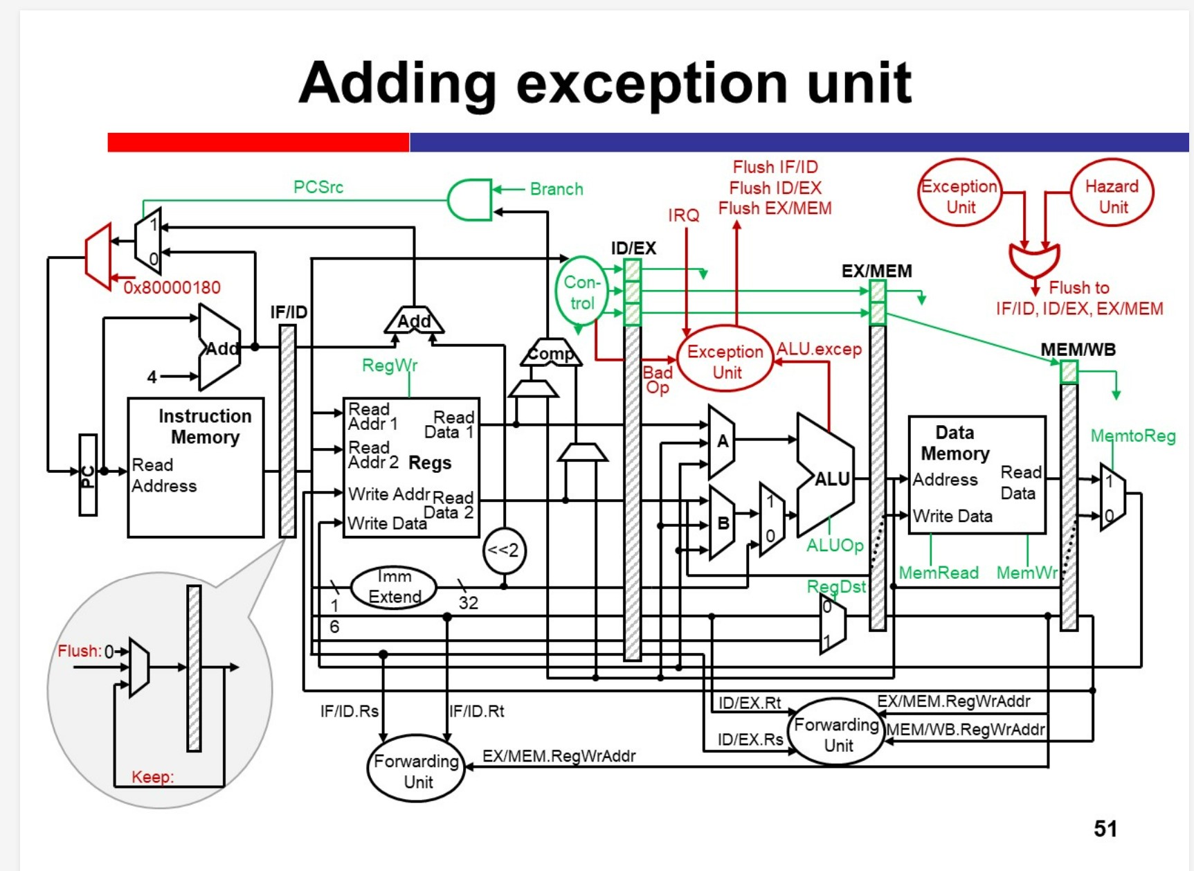
Another type of control hazard: exceptions and interrupts.
– “Exception” includes any unpredictable events that
can change the normal control flow, which has no
distinction between internal and external.
– “Interrupt” is only used for external events.
Advanced techniques for processor
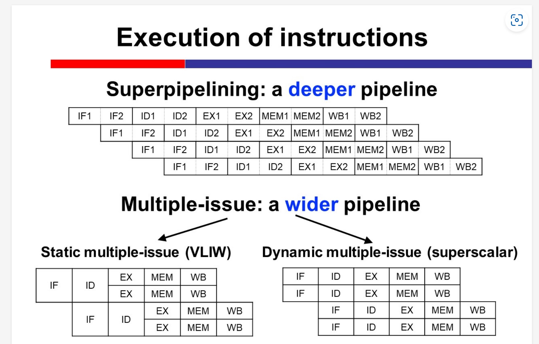
Instruction-level parallelism
Superpipelining: a deeper pipeline
VLIW
Multiple-issue: a wider pipeline
Superscalar
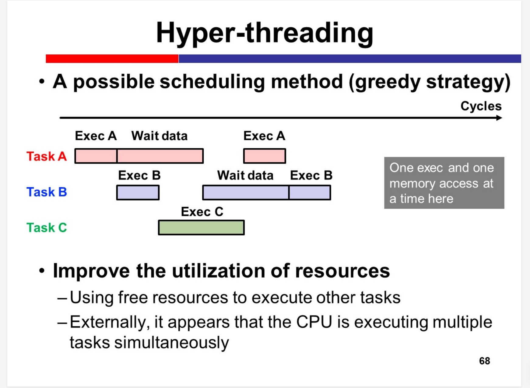
Thread-level parallelism
Hyper-threading
Multicore
Heterogeneous computing
GPU
XPU
Memory
Basics
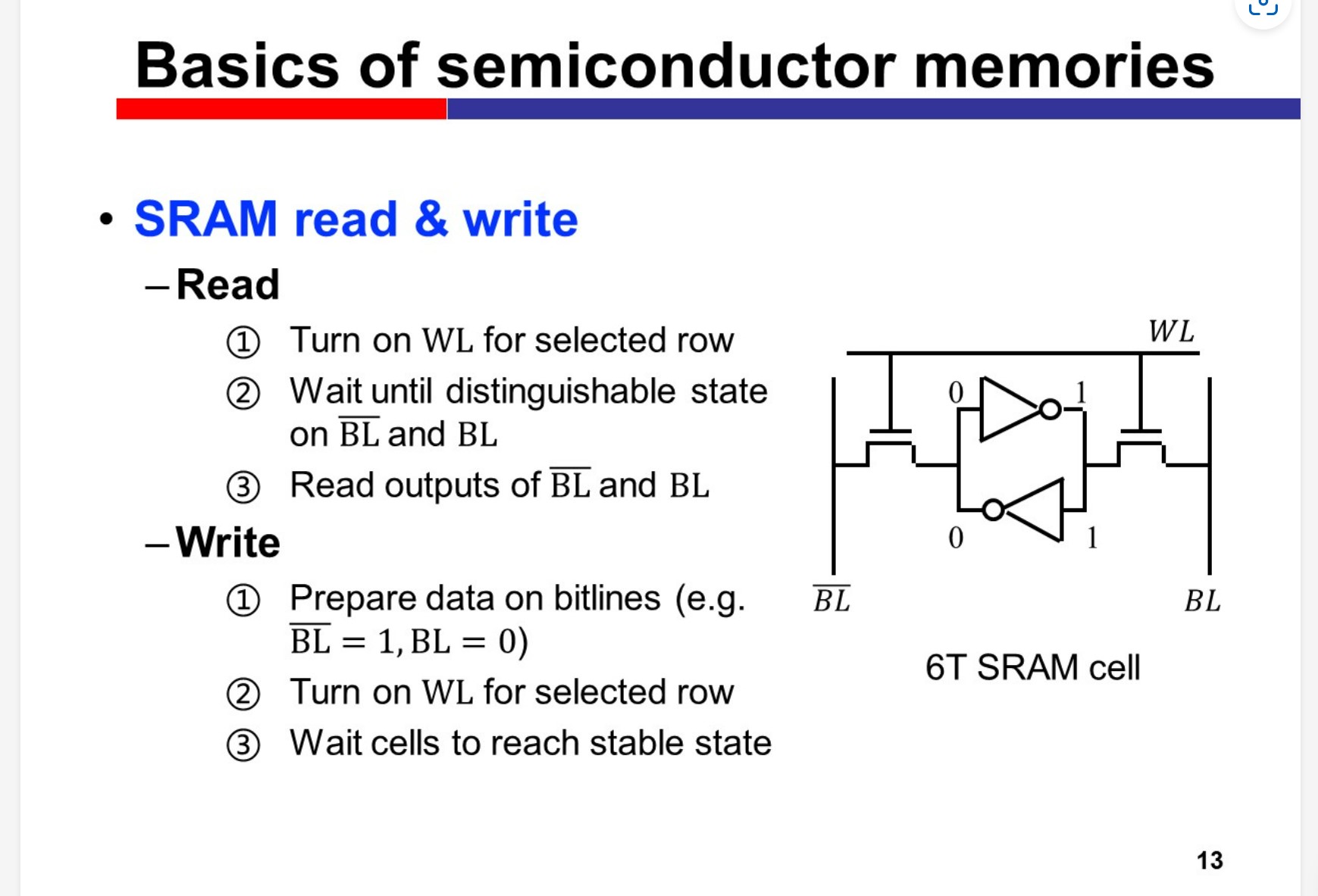
SRAM cell
High speed, low density & expensive
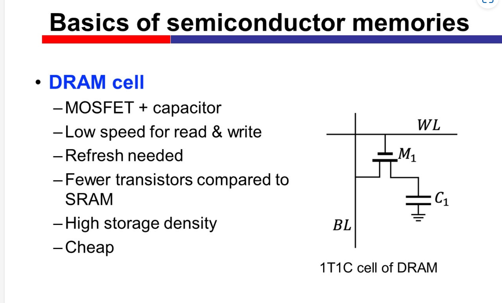
DRAM cell
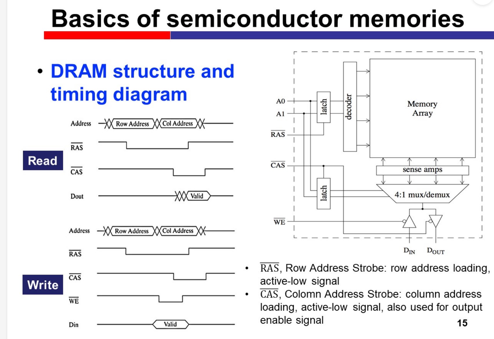
Low speed, high density & cheap. The charge in capacitor may leak, so the data cannot be stored for a long time.
Evaluation
3C model:
Compulsory miss first access to a block
Capacity miss all lines in cache are used
Conflict miss(collision miss) not fully filled, but the blocks # > available ways #.